VOGONS


First post, by feipoa

User metadata
Rank l33t++
Rank
l33t++

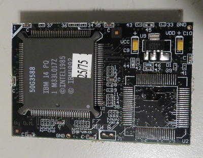
It has been demonstrated elsewhere that the circuitry on the various 386 BL3 upgrade modules can cause issue on many 386 systems. Such modules shown here, download/file.php?id=43450&mode=view

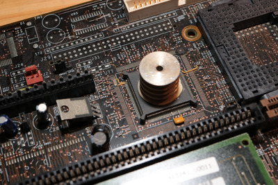
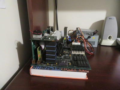
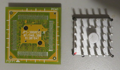
It was recently shown here Re: 3 (+3 more) retro battle stations that we can take a PGA-132 to QFP-132 interposer and slap on an IBM Blue Lightning BL3, however this runs the BL3 at 5 V, so probably not good for long-term use.

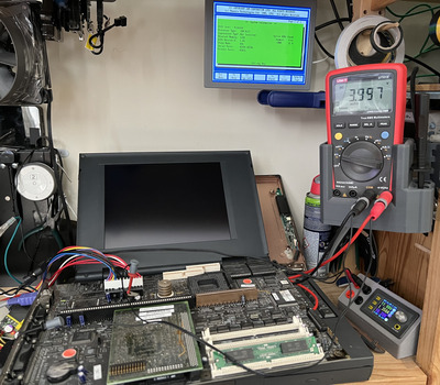
I have begun work to remove the Am386DX from my PGA-132 to QFP-132 interposer and to remove the BL3 from one of my IODATA modules. I know the BL3 in the this particular IODATA module will work up to 110 MHz, albeit with flushing the cache every I/O.

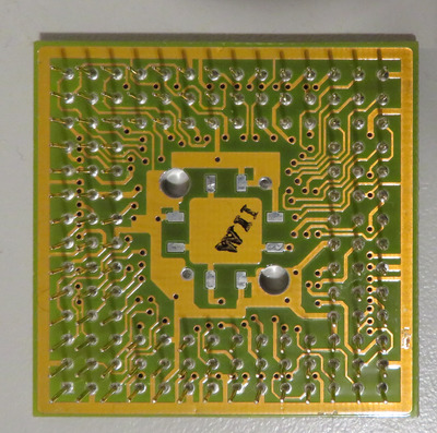
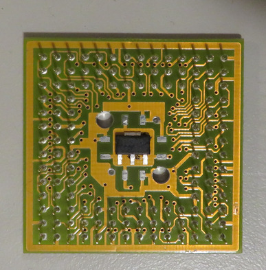
In the photos, I'm showing the top (QFP) and bottom (PGA) of my interposer. On the top face, the centre region has a 5V Vcc plane. On the bottom, the centre square is the GND plane, with a 5V Vcc plane surrounding it. 13 of the 15 Vcc pins on the QFP side are connected to to that centre power plane, while 2 pins are connected to the power plane on the bottom through a via.

PGA132_to_QFP132_top.JPG
Filename
PGA132_to_QFP132_top.JPG
File size
858.92 KiB
Views
1765 views
File license
CC-BY-4.0
PGA132_to_QFP132_bottom.JPG
Filename
PGA132_to_QFP132_bottom.JPG
File size
989.65 KiB
Views
1765 views
File license
CC-BY-4.0
PGA132_to_QFP132_with_BL3.JPG
Filename
PGA132_to_QFP132_with_BL3.JPG
File size
570.56 KiB
Views
1765 views
File license
CC-BY-4.0

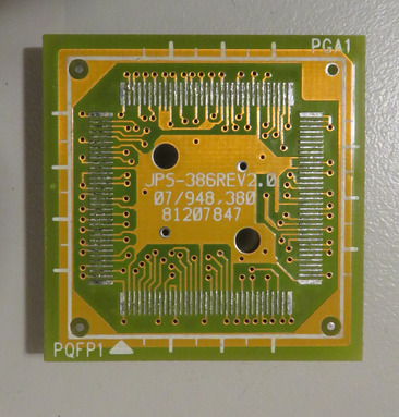
I would like to separate these two power planes so that I can re-purpose them for use with an AMS1117-ADJ voltage regulator and run the BL3 between 3.3 and 4.3 volts. Can this separation be accomplished by drilling out the 11 vias circled in red? The PGA pins look to be surface mounted and I don't think there's any inner traces.

PGA132_to_QFP132_bottom_vias_to_drill.JPG
Filename
PGA132_to_QFP132_bottom_vias_to_drill.JPG
File size
996.48 KiB
Views
1765 views
File license
CC-BY-4.0

Once drilled out, I would place the VRM on the bottom surface and wire it up. To get VRM's Vout to the top QFP layer's power plane, I was thinking to run 4 wires through the 4 larger vias and solder it to the power plane on the top. This would then be 3V Vcc rather than 5V. I'd probably glue a 1K trimmer to the top of the chip for adjustment. I'd also have to run the trimmer's wires though one of the large vias. The regulator's Cin and Cout would also go on the bottom side, alone with R1.

PGA132_to_QFP132_with_AMS1117_ADJ.JPG
Filename
PGA132_to_QFP132_with_AMS1117_ADJ.JPG
File size
602.92 KiB
Views
1765 views
File license
CC-BY-4.0
Last edited by feipoa on 2022-10-06, 21:03. Edited 1 time in total.

Plan your life wisely, you'll be dead before you know it.

Reply 1 of 152, by snufkin

User metadata
Rank Oldbie
Rank
Oldbie

I don't know enough to comment much and haven't even looked up any pinouts, but I'm assuming you've already spotted that pins 85 & 99 on the QFP side aren't fed from the central power area, but from a couple of the vias from the PGA side that are going to be drilled out? Might be better the cut the traces from the pins that feed those traces. One of them is a thin trace anyway, so it won't be providing much current. Don't know what the current requirements are, but are there any heat issues for a voltage regulator there? It'll be burning 2W/Amp.

Reply 2 of 152, by feipoa

User metadata
Rank l33t++
Rank
l33t++

Thank you for checking. I really appreciate the feedback. I hadn't yet decided what to do about pins 85 and 99. I was thinking about drilling the vias and leaving them unconnected. Alternately, I could connect these pins to the top layer power plan with a 30 AWG wire. I've already confirmed that the wire will fit under the BL3 since the IC sits up off the floor like a table with 132 legs.

I'm not sure how much current the BL3 will draw. I couldn't locate any spec sheets. I'd guess around 500 mA max. Perhaps that is too much to be buried on the bottom like this? I originally was going to place the VRM on the top surface but moved it to the bottom for convenience of connections. Should I go back to that approach? The fan from the heatsink will illicit some cooling to the regulator if the regulator is on the top.

Plan your life wisely, you'll be dead before you know it.

Reply 3 of 152, by pshipkov

User metadata
Rank Oldbie
Rank
Oldbie

I am unclear about something.
Datasheets for BL3 are not available.
User @ph4nt0m mentioned in a reply in the linked 3+3 thread that BL3 is 3.3V design, but i am not sure about that.
The chip gets super hot in Alaris Cougar motherboard which is specifically designed for BL3.
With that said - i have to measure the CPU voltage there first before say more.
My point is that - i am unsure about the CPU voltage requirements to start designing something around it 😀

retro bits and bytes

Reply 4 of 152, by feipoa

User metadata
Rank l33t++
Rank
l33t++

I’m pretty sure I’ve measured this before on an adaptor. It was running at 3.35 or 3.45 volts. Probably even at rated voltage it gets hot given enough time or MHz.

Plan your life wisely, you'll be dead before you know it.

Reply 5 of 152, by Thermalwrong

User metadata
Rank Oldbie
Rank
Oldbie

I just took some snaps of my currently homeless IBM Blue Lightning 2/3 (has options for both in BIOS) LPX board, since that might help for determining how much power it needs?
Checking the pins, the LT1085CT regulator is fed from the 5v rail, with the 50v 22uf connecting the regulator's V-IN.
The output pin is connected to that 16v 470uf cap and I'm pretty sure that's the 3.3v output though I haven't measured that while it's on and I've already put it away again 😀
I think that the regulator might be somewhat over-rated for the job but that could be for lack of cooling capacity in its original case.

Attachments

Reply 6 of 152, by Sphere478

User metadata
Rank l33t++
Rank
l33t++

Rather than ruining old hardware, let’s just make a pcb for it?

Sphere's PCB projects.
-
Sphere’s socket 5/7 cpu collection.
-
SUCCESSFUL K6-2+ to K6-3+ Full Cache Enable Mod
-
Tyan S1564S to S1564D single to dual processor conversion (also s1563 and s1562)

Reply 7 of 152, by pshipkov

User metadata
Rank Oldbie
Rank
Oldbie

Ok then. I am convinced. Thanks for the info.

Doing so many tweaks in such a small area that is further confined by CPU socket, cooling, etc., - you will need a really good plan in place and little room for error during work.
I don't know. Personally i wouldn't do it if don't have at least 2-3 more of these adapters.

Sphere's suggestion is more reasonable to me.

retro bits and bytes

Reply 8 of 152, by feipoa

User metadata
Rank l33t++
Rank
l33t++

If someone else wants to create an adapter, I'm OK with that. However, the issue you will run into is that the leads of the footprint of the QFP132's leads will run over the through-hole PGA132 pins. The existing QFP-PGA adapters get around this using surface mount PGA pins. I don't know how to surface mount PGA pins on a PGA with my existing equipment, but if someone else can do it, they can create the adaptor. Alternately, to use through-hole PGA132 pins, the QFP132 would have to be mounted off to the side, which creates a problem with mounting, parasitics, etc. This is what happens for side-by-side configurations: download/file.php?id=146785&mode=view

EDIT: one other idea would be use a PGA132 socket and surface mount it to the PCB using solder paste. However, I don't have the equipment to do this without melting the ABS on the socket.

Plan your life wisely, you'll be dead before you know it.

Reply 9 of 152, by Sphere478

User metadata
Rank l33t++
Rank
l33t++

Brainstorm the design, come up with a plan, and I can help again if you need 😀 this is probably a simpler project than the last one.

There is such a thing as a blind via. But idk who supports making those. Manufacturer wise

Basically you could use thru hole pins that didn’t go all the way through and still be free to smd on the back side.

But I think we will probably come up with a better plan. Honestly, if you can source the smd pins it might be fine to just try and replicate the oem setup. You can use a lif to hold the pins one row at a time and solder them I think.

Gather your info, make sketches, form a plan and I’ll help 😀

Sphere's PCB projects.
-
Sphere’s socket 5/7 cpu collection.
-
SUCCESSFUL K6-2+ to K6-3+ Full Cache Enable Mod
-
Tyan S1564S to S1564D single to dual processor conversion (also s1563 and s1562)

Reply 10 of 152, by feipoa

User metadata
Rank l33t++
Rank
l33t++

A blind via, is that a via which doesn't penetrate through to the other side? If so, that might work if the via is wide enough to accommodate a machine pin. Without a valley for the machine pin to sit in, I wouldn't trust the surface mount machine pins for any length of time.

Another of the larger hurtles for this particular design is that we don't have access to cheap NOS IBM BL3 chips. Anyone who has an interposer or motherboard with a BL3 will have to sacrifice a $300 piece of hardware to pull the BL3 off. So the benefit of such a design won't be nearly as widespread as the SXL2 interposer, for which there seem to be hundreds of accessible NOS SXL2-66 chips for $18 each.

Plan your life wisely, you'll be dead before you know it.

Reply 11 of 152, by snufkin

User metadata
Rank Oldbie
Rank
Oldbie

From Thermalwrong's photos then it looks like R2 and R3 are probably the divider for the 1085 as I think they connect to the adjust pin (1). Output is 1.25*(1+resistor to ground/resistor to Vout). I think the blue resistor (R2) goes to ground (big trace to via), so guess that R3 goes to Vout. R3 is a 120 ohm resistor and R2 looks like it says 270R. So 1.25*(1+270/120)=4.06V.

Strange voltage. Entirely possible I've guessed wrong. Also interesting in the photos to see the extra decoupling caps that have been added to the CPU pins. If they were undervolting it then it could indicate they needed extra smoothing to make it stable.

Assuming Vout is 4V and Vin is 5V, then that TO220 package is burning 1W/Amp. Thermal resistance is probably around 75C/W (no heatsink, so just case to ambient). Maximum temperature is around 125C. So maximum power burnt in the regulator is 125/75=1 2/3W. So the CPU can't be drawing any more than a bit over 1.5A max. I'd worry about any linear regulator sandwiched between motherboard and CPU PCB.

Blind vias used to get expensive and I'm not sure how much they'd help with trying to solder pins in place as they'd need to be put in place before the top layer of the PCB was laminated on. I wonder if it would be possible to do a home-made PCB sandwich? Have pads that line up when 2 PCBs are placed face-to-face, or pads that line up with the flange base of through-hole pins. Squeegee on some solder paste, put them together and heat them up. Kind of like BGA components, except the component is a PCB.

Just realised I mentioned sandwich twice there. Lunchtime I think.

Reply 12 of 152, by feipoa

User metadata
Rank l33t++
Rank
l33t++

Best way to determine the running voltage is to measure it.

I've measured it in 4 adaptors, however the results are mixed.

My Buffalo BL3-75 with the computer turned on is measuring 4.14 V.

Buffalo_BL3-75_in_computer_4.14V.JPG
Filename
Buffalo_BL3-75_in_computer_4.14V.JPG
File size
238.19 KiB
Views
1567 views
File license
CC-BY-4.0

My IODATA BL3-75 without any CPU (I've already desoldered it) is measuring 3.79 V.

IODATA_BL3-75_no_CPU_3.79V.JPG
Filename
IODATA_BL3-75_no_CPU_3.79V.JPG
File size
213.45 KiB
Views
1567 views
File license
CC-BY-4.0

My IODATA BL3-60 with CPU is measuring 3.47 V.

IODATA_BL3-60_with_CPU_3.47V.JPG
Filename
IODATA_BL3-60_with_CPU_3.47V.JPG
File size
300.49 KiB
Views
1567 views
File license
CC-BY-4.0

My Evergreen BL3-75 with CPU is measuring 3.58 V. Notice how the Evergreen unit is also using the 1117 VRM, which has a max output current of 800 mA.

Evergreen_BL3-75_3.58V.JPG
Filename
Evergreen_BL3-75_3.58V.JPG
File size
235.26 KiB
Views
1567 views
File license
CC-BY-4.0
Evergreen_BL3-75_using_1117_VRM.JPG
Filename
Evergreen_BL3-75_using_1117_VRM.JPG
File size
814.18 KiB
Views
1567 views
File license
CC-BY-4.0

I may very well put the VRM on the top surface. I had photos of this configuration that I posted in another thread months ago, but I can no longer find the photos. Given the variance in voltages, I'll be implementing a trim pot. 3.5 V to 4.15 V seems like a large range. I wonder if the upgrade companies adjusted the running voltage to account for low chip yields. I know my IODATA with BL3-60 will not do over 75 MHz, while the BL3-75 will go to 110 MHz.

For those who have a motherboard with a BL3 installed, could you measure the CPU's running voltage.

Plan your life wisely, you'll be dead before you know it.

Reply 13 of 152, by Sphere478

User metadata
Rank l33t++
Rank
l33t++

A bga stack occurred to me but seemed too complicated. I mean if someone had mad bga skills sure, it’s possible. But it seems like just using smd pins would be easier.

Sphere's PCB projects.
-
Sphere’s socket 5/7 cpu collection.
-
SUCCESSFUL K6-2+ to K6-3+ Full Cache Enable Mod
-
Tyan S1564S to S1564D single to dual processor conversion (also s1563 and s1562)

Reply 15 of 152, by Thermalwrong

User metadata
Rank Oldbie
Rank
Oldbie

Huh, I didn't realise that multiple Blue Lightning CPU upgrade boards used the AMS1117. It probably requires using the PCB's copper and the SMD mounting to dissipate heat.
I think the LT1085CT was picked on mine for lack of cooling since a 7.5 amp linear regulator is quite over-rated for a CPU that's kind of suited towards mobile use.

I can try out my BL3 board and check the voltage tomorrow if it could help.
For the PCB design if that's an option (I think that's better than modifying the existing board, personally) - just copying one of the better adapters would probably be best if it doesn't require glue logic and hopefully isn't 4 layer.
And well, if it is 4 layer or more layers, that's possible to copy too, just destructively unless you have an x-ray setup handy.

Reply 16 of 152, by Sphere478

User metadata
Rank l33t++
Rank
l33t++

We can probably extrapolate a passive interposer using pinout for the socket and datasheet for the chip even if the oem are 4 layer

Sphere's PCB projects.
-
Sphere’s socket 5/7 cpu collection.
-
SUCCESSFUL K6-2+ to K6-3+ Full Cache Enable Mod
-
Tyan S1564S to S1564D single to dual processor conversion (also s1563 and s1562)

Reply 17 of 152, by Thermalwrong

User metadata
Rank Oldbie
Rank
Oldbie

Pulled it out and plugged it back into the test setup briefly, it does run at 4 volts 😀

Attachments

Reply 18 of 152, by feipoa

User metadata
Rank l33t++
Rank
l33t++

Thanks. The voltages are all over the place! Kind of reminds me how Cyrix would qualify the same CPUs at different voltages.

Plan your life wisely, you'll be dead before you know it.

Reply 19 of 152, by feipoa

User metadata
Rank l33t++
Rank
l33t++

Something that would be more useful than a custom BL3 adapter that only, say, 5 people at most would might use, would be a PGA-132 rotation interposer. Very rarely am I able to insert a 386 upgrade adapter without having to lift it up with sockets to meet some clearance. The worst example I've come across is with my BL3-75 system , which required 2-dozen sockets to clear a VLB card. With a rotation interposer, I could avoid this entirely.

If you are looking to assist in other custom PCBs, I would suggest a PGA-132 rotator socket. Just take every pin on the PGA-132 and rotate it perpendicularly. There are 3 rotations (thus 3 different PCBs) which would be needed to complete a full circle, one at +90 degrees rotated, another at 180 degrees, and one at -90 degrees rotated. You could intertwine the sockets like you did with the recent SXL2 interposer.

Attachments

Plan your life wisely, you'll be dead before you know it.