VOGONS


PGA132 rotator boards

Topic actions

Reply 40 of 116, by feipoa

User metadata
Rank l33t++
Rank
l33t++
Sphere478 wrote on 2022-12-04, 06:29:

I’m routing in 6 layer for my attenpt.

Yes, two surface mount.

Unfortunately this means every pad will have two vias beside it. I can cover them with silk though.

As they say in mandarin, "jia you"!

This is 180 degrees with ground plane?

Plan your life wisely, you'll be dead before you know it.

Reply 41 of 116, by snufkin

User metadata
Rank Oldbie
Rank
Oldbie
Sphere478 wrote on 2022-12-04, 06:29:

Unfortunately this means every pad will have two vias beside it. I can cover them with silk though.

Can tented vias (solder resist over the top of the via) be used?

Reply 42 of 116, by Sphere478

User metadata
Rank l33t++
Rank
l33t++

90*

Not sure, how do I do a tented via in kicad? Or is it a option when ordering?

Sphere's PCB projects.
-
Sphere’s socket 5/7 cpu collection.
-
SUCCESSFUL K6-2+ to K6-3+ Full Cache Enable Mod
-
Tyan S1564S to S1564D single to dual processor conversion (also s1563 and s1562)

Reply 43 of 116, by maxtherabbit

User metadata
Rank l33t
Rank
l33t
Sphere478 wrote on 2022-12-04, 16:06:

90*

Not sure, how do I do a tented via in kicad? Or is it a option when ordering?

I believe you just go to its properties and change type to blind/buried. As long as the correct copper layers are selected it should do what you want

Reply 44 of 116, by Sphere478

User metadata
Rank l33t++
Rank
l33t++

Ah blind buried isn’t supported by jlcpcb

Sphere's PCB projects.
-
Sphere’s socket 5/7 cpu collection.
-
SUCCESSFUL K6-2+ to K6-3+ Full Cache Enable Mod
-
Tyan S1564S to S1564D single to dual processor conversion (also s1563 and s1562)

Reply 45 of 116, by maxtherabbit

User metadata
Rank l33t
Rank
l33t
Sphere478 wrote on 2022-12-04, 19:14:

Ah blind buried isn’t supported by jlcpcb

You sure? I know for certain they don't let you bury them under copper layers - but if you set the type to blind/buried and choose the outtermost coppers as start and finish it should pass DRC

Alternatively you just manually edit the solder mask layer with a zone

Reply 46 of 116, by Sphere478

User metadata
Rank l33t++
Rank
l33t++

I believe vias don’t have any solder mask clearance. In other words the varnish should already be over them. Problem is that it isn’t always enough.

Sphere's PCB projects.
-
Sphere’s socket 5/7 cpu collection.
-
SUCCESSFUL K6-2+ to K6-3+ Full Cache Enable Mod
-
Tyan S1564S to S1564D single to dual processor conversion (also s1563 and s1562)

Reply 47 of 116, by feipoa

User metadata
Rank l33t++
Rank
l33t++

If it is going to be 6-layer, I'd suggest starting with 180 degrees.

I contacted JLCPCB a few weeks ago and they do not support blind vias.

Plan your life wisely, you'll be dead before you know it.

Reply 48 of 116, by Sphere478

User metadata
Rank l33t++
Rank
l33t++

Already pretty far into 90* if I settle on a routing pattern for the outer ring the inner rings should fall into place

Sphere's PCB projects.
-
Sphere’s socket 5/7 cpu collection.
-
SUCCESSFUL K6-2+ to K6-3+ Full Cache Enable Mod
-
Tyan S1564S to S1564D single to dual processor conversion (also s1563 and s1562)

Reply 49 of 116, by Sphere478

User metadata
Rank l33t++
Rank
l33t++

Btw my current attempt is a pin tor pin woth no distinction for power and ground. Just a 90* twist of every single pin

Sphere's PCB projects.
-
Sphere’s socket 5/7 cpu collection.
-
SUCCESSFUL K6-2+ to K6-3+ Full Cache Enable Mod
-
Tyan S1564S to S1564D single to dual processor conversion (also s1563 and s1562)

Reply 50 of 116, by feipoa

User metadata
Rank l33t++
Rank
l33t++

I suppose if you create all 3 rotations before prototyping, it shouldn't be an issue. Due to the cost involvement with 6-layer, I would start testing with 180 degrees. Once it is determined that 180 degrees works, I won't be ordering the 90 degree and 270 degree units unless I run into an application which demands it, but I would keep the gerbers handy for the situation. The $85 cost is too high to order something before I need it, and right now I need 180 degrees. If 180 degrees works, then the other two orientations will likely work.

I gently alluded to this earlier,

feipoa wrote on 2022-11-04, 22:54:

For one such motherboard I have setup at present, the 180 degree orientation is the one it needs. However, I have run into this issue on a few motherboards.

Given the issue with possible VCC plane on the SXL2 interposer, I think a direct rotation of every pin might offer some further insight. I can even run the rotator board with the same SXL2-66 CPU using the Improve It + Gainbery and check for higher than expected noise.

Plan your life wisely, you'll be dead before you know it.

Reply 51 of 116, by feipoa

User metadata
Rank l33t++
Rank
l33t++

If there's a way to force the 90 degree into 4-layer, then the situation is much better and we can experiment with the noise in greater depth for a fraction of the cost. But at 6-layer, to experiment, even with the 180 degree unit, one with no GND/Vcc plane, and another with all pins directly mapped, that will cost around $170 USD. If 90-degree cannot be 4-layer, then we should really start with 180 degree.

Plan your life wisely, you'll be dead before you know it.

Reply 52 of 116, by Sphere478

User metadata
Rank l33t++
Rank
l33t++

So let me remind that this is a non offset attempt. Smd design.

I’m coming up one pin short 🤣.

I’m starting with the outer layer of course because it is the hardest. But it is making it pretty apparent that doing it in a organized way is kinda hard. Here is my latest routing pattern. I have managed to route all but one. I think perhaps if I shift half of each side toward center I can make another ring on the outside to route the corners.

Attachments

  • image.jpg
    Filename
    image.jpg
    File size
    1.52 MiB
    Views
    623 views
    File license
    Public domain

Sphere's PCB projects.
-
Sphere’s socket 5/7 cpu collection.
-
SUCCESSFUL K6-2+ to K6-3+ Full Cache Enable Mod
-
Tyan S1564S to S1564D single to dual processor conversion (also s1563 and s1562)

Reply 53 of 116, by Sphere478

User metadata
Rank l33t++
Rank
l33t++

Success!

Unfortunately this leaves a huge question mark for the middle ring. I don’t think there are is enough space left for middle with only two paths.

Attachments

  • image.jpg
    Filename
    image.jpg
    File size
    1.9 MiB
    Views
    622 views
    File license
    Public domain
Last edited by Sphere478 on 2022-12-29, 18:06. Edited 1 time in total.

Sphere's PCB projects.
-
Sphere’s socket 5/7 cpu collection.
-
SUCCESSFUL K6-2+ to K6-3+ Full Cache Enable Mod
-
Tyan S1564S to S1564D single to dual processor conversion (also s1563 and s1562)

Reply 54 of 116, by Sphere478

User metadata
Rank l33t++
Rank
l33t++

Sorry feiopa, I had already started with 90.

Kinda on a roll.

I’ll try to get to the others.

I’m trying to find a elegant way to do this, I don’t want it to be spaghetti. :p

Sphere's PCB projects.
-
Sphere’s socket 5/7 cpu collection.
-
SUCCESSFUL K6-2+ to K6-3+ Full Cache Enable Mod
-
Tyan S1564S to S1564D single to dual processor conversion (also s1563 and s1562)

Reply 55 of 116, by Sphere478

User metadata
Rank l33t++
Rank
l33t++

Outer and middle row routed. Middle should be easy now.

6 layer, ‘in place’, SMD, 90*

2 stacked bga style for 180*?

Attachments

  • image.jpg
    Filename
    image.jpg
    File size
    1.78 MiB
    Views
    574 views
    File license
    Public domain

Sphere's PCB projects.
-
Sphere’s socket 5/7 cpu collection.
-
SUCCESSFUL K6-2+ to K6-3+ Full Cache Enable Mod
-
Tyan S1564S to S1564D single to dual processor conversion (also s1563 and s1562)

Reply 56 of 116, by feipoa

User metadata
Rank l33t++
Rank
l33t++

I won't be available much until the kids are back in school.

You were able to do +90 degrees as 6-layer? Your latest PM suggested 8-layer was required.

Can 180 degrees be done 8-layer, SMD both sides?

Worse case, you could always start increase the size of the PCB, perhaps starting with 1 mm all around.

Plan your life wisely, you'll be dead before you know it.

Reply 57 of 116, by Sphere478

User metadata
Rank l33t++
Rank
l33t++
feipoa wrote on 2022-12-28, 14:40:
I won't be available much until the kids are back in school. […]
Show full quote

I won't be available much until the kids are back in school.

You were able to do +90 degrees as 6-layer? Your latest PM suggested 8-layer was required.

Can 180 degrees be done 8-layer, SMD both sides?

Worse case, you could always start increase the size of the PCB, perhaps starting with 1 mm all around.

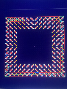
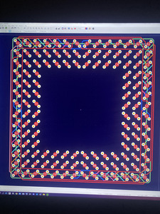
Yes, I thought it wasn’t going to work, but I figured it out on pink layer. See the squiggly on pink?

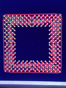
Of course I could cheat and throw more vias everywhere, and make spaghetti but am trying to do it in a organized way.

This adapter is a clusterhump for signal interference btw.. The other approaches also, it looks like. So if it works at 80mhz that will be very interesting.

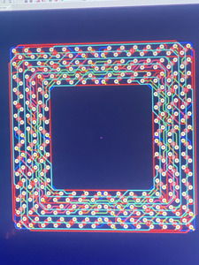
If we want to do something for that, we could go 10 or 12 layer and put ground planes between all layers. That would probably help. Then do bga stack for 180

It may be possible to route on less layers and fit ground planes between if we abandon the organized approach and throw more vias everywhere. But I still think that would be 8-10 layer at least and would look nasty 🤣

Idk, pros/cons.

But doing it this way (my way) it seems like 180 would take 12 layer at least. So the obvious solution is bga. This 90* is actually taking quite a bit of time to make. I’ve started over several times but seem to be on a roll with this latest one.

The nice thing is that the traces are almost equal length with this approach btw.

They get longer on the outside and shorter on the inside but the difference isn’t huge.

This is still 1:1 btw

If I went 10-12 layer how much would that be at jlcpcb these days? I know they changed their pricing recently. 🤔 if they can do it affordably adding ground layers might be a good idea.

Little redundant but I’ll also post the reply to the pm here as it kinda clarifies.

Rotator: Perhaps increase PCB size by 1 mm on all sides? Would that help meet 6-layer requirements? If not, and it needs to be 8-layer, that's just how it goes...

Increasing pcb size will only help if more vias are used you can only route so many before traces start to over lap. Jumping over a trace takes 1-2 vias depending. More vias means more length and less signal quality.

At this point I seem to have figured out the problem with routing middle layer. Inner layer should fall into place now and yeild a successful proof of concept for routing this way. The next step is ground plane. And the best way to ground this would probably require 4-6more layers. Because there is basically no chance of propagating ground on the signal layers

Sphere's PCB projects.
-
Sphere’s socket 5/7 cpu collection.
-
SUCCESSFUL K6-2+ to K6-3+ Full Cache Enable Mod
-
Tyan S1564S to S1564D single to dual processor conversion (also s1563 and s1562)

Reply 58 of 116, by Sphere478

User metadata
Rank l33t++
Rank
l33t++

I’m looking at the 132 pga pinout for a intel chip, and unless I am missing something there are no symmetrical vss/gnd locations.

So to ground the ground plane we have two options:

A spring in the middle to the metal lid on the back of the cpu

Or a external ground strap to a mobo screw.

(If we add more layers for ground)

Here is my current plan:

I’m going to silk the whole dang board. Cover all those vias, only holes will be the pads themselves

Then I’m gonna cut out the center and make it a hole, just because that’s how badass compact I’ve made this 🤣.

And finally, unless apposed I’m going to add ground layers and make the pcb edge conductive so that a ground strap can be soldered to it. Or/and may put a suspended spring holder in the middle. Will see.

Sphere's PCB projects.
-
Sphere’s socket 5/7 cpu collection.
-
SUCCESSFUL K6-2+ to K6-3+ Full Cache Enable Mod
-
Tyan S1564S to S1564D single to dual processor conversion (also s1563 and s1562)

Reply 59 of 116, by Sphere478

User metadata
Rank l33t++
Rank
l33t++

Fully routed.

I gotta go back and make sure all the pins are rotating the same direction (easy fix so long as I catch it 🤣)

Then a few passes checking the trace routing for clearance/optimal paths. Also need to add ground layers. I think it would probably be a mistake not to have them.

Attachments

  • image.jpg
    Filename
    image.jpg
    File size
    1.65 MiB
    Views
    503 views
    File license
    Public domain

Sphere's PCB projects.
-
Sphere’s socket 5/7 cpu collection.
-
SUCCESSFUL K6-2+ to K6-3+ Full Cache Enable Mod
-
Tyan S1564S to S1564D single to dual processor conversion (also s1563 and s1562)