First post, by majestyk

Rank
Oldbie
- Rank
- Oldbie
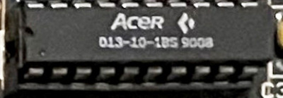
Does anyone here happen to know any details / info about this DIL circuit / chip?
I have never before seen one and cannot find a datasheet or information.
Does anyone here happen to know any details / info about this DIL circuit / chip?
I have never before seen one and cannot find a datasheet or information.
Cache chip?
Might help to see where and on what PCB it's mounted.😄
Might be worth asking in the CPU-World forums, lot of chip collectors, and someone might have details of the in-house part number and know what it is. A few members have stacks of datasheets 😀
See my graphics card database at www.gpuzoo.com
Constantly being worked on. Feel free to message me with any corrections or details of cards you would like me to research and add.
Reminds me of the ALI M5819P RTC, does it get battery power on some pin?
Acer rebranded a ton of stuff, but also had full access to UMC - Taiwans first foundry https://www.youtube.com/watch?v=q55lQUHg7Dg with huge inhouse engineering team producing designs for internal Taiwanese industry consumption.
but most likely something as stupid as rebranded PAL Re: SATA HARD Disk in 286/386 Mobo: Is it possible?
Tbh I suspected it to be some PAL, because it´s missing on my mainboard and for no apparent reason everybody rips out all the PALs (and BIOS of course) before selling their mainboards.
It´s located near the oscillator and next to CPU / FPU so it might be involved in selecting FPU frequency?
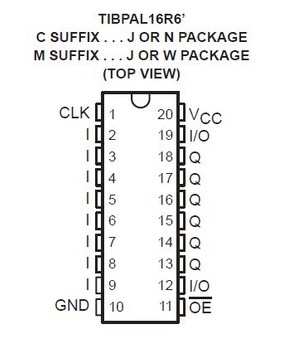
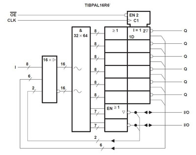
I was unable to find any details about the "ACER" circuit, but I found out that for the same circuit the manufacturer also used the Texas Instruments "TIBPAL 16R6-15CN", a PAL that is well documented.
https://www.digchip.com/datasheets/parts/data … L8-15CN-pdf.php
I also have a working sample of this PAL from a second mainboard.
What do you think would be the easiest way to read it´s data and program a new TIBPAL16R6 or some aequivalent GAL with it?
that R in 16R6 is for registers, afair those are unclonable if programmer used this functionality because logic can fold on itself (feedback)?
on the other hand this dude has a sketch ready for it http://www.vintagecomputer.net/fjkraan/digaud … ad/palread.html but Im dubious about its efficacy
Those guys are serious business cracking old arcades https://github.com/DuPAL-PAL-DUmper/DuPAL_Analyzer https://github.com/DuPAL-PAL-DUmper/DuPAL_Board https://github.com/DuPAL-PAL-DUmper/DuPAL_Ana … ocs/analysis.md
might be easier to reverse engineer the board itself and identify what was this chip function to begin with
We do know (or at least can be quite confident) that a TIBPAL 16R6-15CN can be configured to behave identical to the Acer chip, at least as far as that device is concerned. That doesn't mean it has be be that kind of PAL, it can be any other similar kind of PAL, or one of the successor chips like PEEL or GAL, which are available from different vendors, using different programming and verification methods, which are usually not well documented. It's also not impossible that Acer got an IC manufacturer to build the required logic into a factory-programmed gate array instead of using any kind of electrically programmable gate array. So trying to read that chip might prove difficult to impossible, not only due to copy protection (which can be glitched on some kinds of PALs and GALs).
I tried to gather some more information concerning the integration of this TIBPAL 16R6-15CN.
Here are the connections I found:
Pin1: 48 MHz Output of the quartz oscillator
Pin2 (I): GND
Pin3 (I): VL82C101B pin 7 "-S0"
Pin4 (I): VL82C101B pin 6 "-S1"
Pin5 (I): VL82C101B pin 8 "M/-IO"
Pin6 (I): VL82C101B pin 14 "F16"
Pin7 (I): VL82C101B pin 65 "READY"
Pin8 (I): VL82C101B pin 72 "AEN2"
Pin9 (I): Turbo LED- and - after passing a 7400 NAND gate the Turbo Switch connector
Pin10: GND
Pin11 (OE#): GND
Pin12 (I/O): VL82C101B pin 47 "SysClk" (alo connected to other chips)
Pin13 - Pin17 (Q) "NC"
Pin18 (Q): VL82C101B pin 84 "XTAL2(2)"
Pin19 (I/O): VL82C101B pin 5 "HLDA"
VL82C101B System Controller datasheet:
majestyk wrote on 2023-04-22, 08:25:Pin1: 48 MHz Output of the quartz oscillator Pin2 (I): GND Pin3 (I): VL82C101B pin 7 "-S0" Pin4 (I): VL82C101B pin 6 "-S1" P […]
Pin1: 48 MHz Output of the quartz oscillator
Pin2 (I): GND
Pin3 (I): VL82C101B pin 7 "-S0"
Pin4 (I): VL82C101B pin 6 "-S1"
Pin5 (I): VL82C101B pin 8 "M/-IO"
Pin6 (I): VL82C101B pin 14 "F16"
Pin7 (I): VL82C101B pin 65 "READY"
Pin8 (I): VL82C101B pin 72 "AEN2"
Pin9 (I): Turbo LED- and - after passing a 7400 NAND gate the Turbo Switch connector
Pin10: GND
Pin11 (OE#): GND
Pin12 (I/O): VL82C101B pin 47 "SysClk" (alo connected to other chips)
Pin13 - Pin17 (Q) "NC"
Pin18 (Q): VL82C101B pin 84 "XTAL2(2)"
Pin19 (I/O): VL82C101B pin 5 "HLDA"
EDIT: Fixed the guess after skimming the datasheet.
With this sets of pins, the function of that PAL is quite obvious. It gets the 48 MHz base clock (into the dedicated clock input), and synthesizes the primary clock for the processor/chipset (XTAL2). Probably you miscounted pins by 1, because pin 84 "XTAL2(2)" is an output pin of the chipset, and Pin 18 (Q) is an output pin of the PAL. Pin 83 "XTAL2(1)" would be the pin that can receive an externally generated primary clock. The 286 requires two times the operating frequency at its CLK2 input (that's why there is the 2 in the pin name). For 12MHz operation, XTAL2(1) needs to receive 24MHz, which is easily generated from the 48 MHz input clock by dividing it by 2.
As this chipset uses a synchronous ISA design, the ISA bus clock is just XTAL2/2, which would result in 12MHz bus clock. This fequency is considered too high for good ISA compatibility; so during ISA access, XTAL2 should be 16 MHz instead of 24MHz, running the processor at 8MHz, which is a perfect match for the ISA bus. You easily get 16MHz from 48MHz as well, by dividing the clock by 3.
Furthermore, there is a Turbo input that likely forces the processor clock to be 8MHz all the time (or possibly 6MHz by using 4 as divider).
All the other inputs (including SYSCLK which is generated from the XTAL2 input by the chipset) are used to monitor bus activity. If the processor accesses an address that is located on the ISA bus, the (double) processor clock output will be 16MHz, if the processor does not actively access the ISA bus, and Turbo is enabled, the clock output will be 24MHz.
Thanks for all the clues!
The 82C101B also has it´s own oscillator (14.31818 MHz) connected to "XTAL1(1)" and "XTAL1(2)".
Pin 1 is ground and the next pin right of pin 1, pin 84 XTAL2(2) is definitely routed to pin 18 of the 16R6.
When there are 2 pins at a chip to connect a crystal that drives the oscillator inside the chip and if you choose not to use a crystal, but feed an external oscillator signal to the circuit, I have seen several cases when you could use either pin for the signal and ground the other one / or let it float. Couldn´t this be the case here?
majestyk wrote on 2023-04-22, 13:25:When there are 2 pins at a chip to connect a crystal that drives the oscillator inside the chip and if you choose not to use a crystal, but feed an external oscillator signal to the circuit, I have seen several cases when you could use either pin for the signal and ground the other one / or let it float. Couldn´t this be the case here?
Typically, the oscillators integrated in ICs are Pierce oscillators, with the inverter and the resistor already integrated in the chip, and you having to add the two capacitors and the crystal externally. In a Pierce oscillator, you are supposed to inject an external clock at the input side of the integrated inverter. If the clock signal is sufficiently strong, you might be successful injecting it at the output side of the inverter, too, but in that case, you are fighting the inverter that tries to pull the input to a center point. This is usually considered bad design. As Wikipedia goes on, it is recommended to have a series resistor at the inverter output (which basically increases the inverter output impedance), so the inverter isn't able to pull very hard, which makes it easier to inject an external clock signal. Nevertheless, fighting the inverter at its output instead of feeding it at its input is considered bad design.
To me, this means one of two things: Either the datasheet got the "input" and "output" designations of XTAL2 mixed up (it is quite clear on pin 83 being the input and pin 84 being the output), or there is a design flaw on the board that wasn't caught by any kind of quality control, because it works even with that flaw.
I have a second mainboard with the same chipset and similar, but not identical layout. It also connects pin 18 of the 16R6 with pin 84.
This could be due to the fact that the datasheet has an error here, or, because the copycats were working overtime back then in Taiwan copying designs and layouts, they blindly copied slightly flawed designs as well.
I noticed the sticker on your picture of PAL. Did you eventually create a working clone of it?