Reply 40 of 71, by RayeR
- Rank
- Oldbie
Thanks for effort, thankfully my vision is still sharp enough to see this pins w/o mag. lens 😀
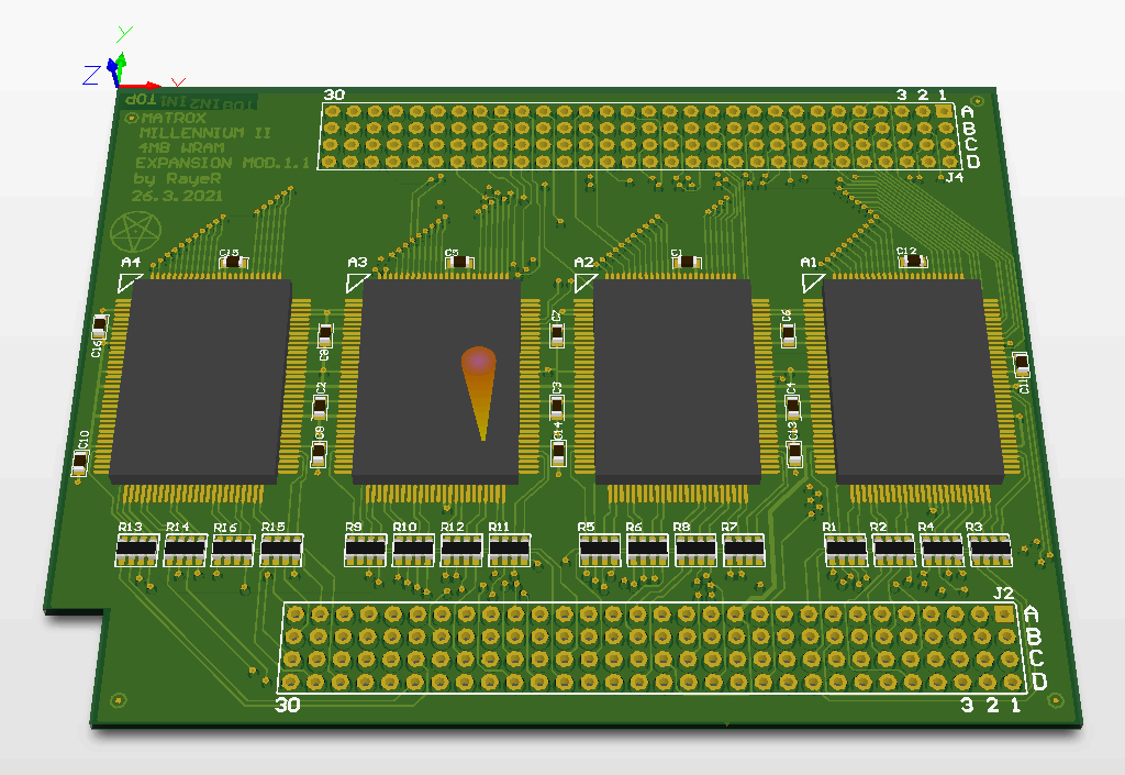
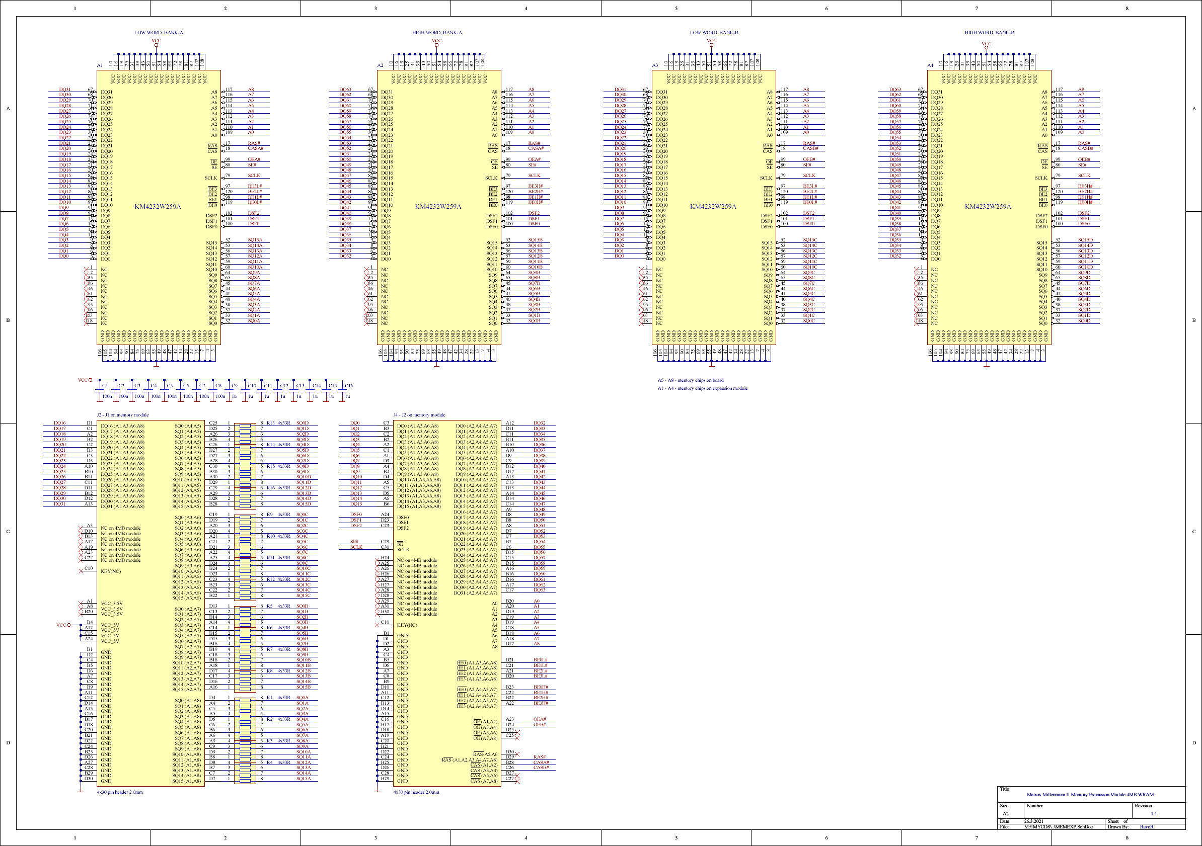
Now we have important OE and CAS signals that are grouped by 2 chips for 64b data bus width, but I'm missing the RAS. I belive it should have 2 separate pins as CAS has. You probably missed it but try also J4-D30 and J4-D29 that are RAS of onboard chips.
I wonder a bit about J4 A23 that is connected with B30 on the card but not on module, maybe used on 12MB version.
Also I need to figure data bus mapping so please check at least J4-A12 (DQ0) and J4-C3(DQ0) which goes to what chips (pin 5 on mem.chip)
and similar for J4-D21,C21,A21,D20 (BE0-3) and J4-B23,C22,B22,A22 (BE0-3) which goes to what chips (pins 119, 98, 120, 97 on mem. chip)
Also not clear about SQ0-15 lines that each onboard chip have them separate but I guess it would be also separately connected to 4 mem chips. on module, so please check at least J2-C25(SQ0), J2-C19(SQ0), J2-D13(SQ0), J2-D4(SQ0) which goes to what chips (pin 32 on mem. chip). This pins seems to have 33ohm resistors in series so be sure your DMM beeps at this resistance yet.
Gigabyte GA-P67-DS3-B3, Core i7-2600K @4,5GHz, 8GB DDR3, 128GB SSD, GTX970(GF7900GT), SB Audigy + YMF724F + DreamBlaster combo + LPC2ISA

