VOGONS


New clock gen for tyan s1564d (Research)

Topic actions

Reply 40 of 105, by stamasd

User metadata
Rank l33t
Rank
l33t

It would need an interposer of course, to adapt to the other chip's pinout. Or make custom boards for the DDS instead of using the premade dev boards, but that would be more expensive. Those dev boards are very handy and not too expensive, you can find them around $20 each. I've used them in several projects where I needed custom signal generators.

Do note that those generate only 1 frequency at a time, and if you need separate signals at the same time (like the keyboard clock) you have to generate them using supplemental circuitry.

I/O, I/O,
It's off to disk I go,
With a bit and a byte
And a read and a write,
I/O, I/O

Reply 41 of 105, by snufkin

User metadata
Rank Oldbie
Rank
Oldbie

I think we've worked out that there are 4 frequencies needed: PClk (processor clock), BClk (needs to be in phase with and /2 PCLK), 24MHz (for chipset stuff) and a reference (14.318MHZ). Sphere checked before that the KBC runs ok from the reference clock. The existing clock gen has 4 PClk outputs and 6 BClk outputs, so the outputs from any other clock source would probably need to be buffered to drive those cleanly. Although it's possible that not all the outputs are actually used. Easiest way to check which outputs are used would be to lift the existing clock gen and see which outputs are routed out.

Might be able to get away with generating BClk by passing PClk through a flip-flop, but it might be tricky to keep them in phase (might need radiators on the PClk to slow it down a little).

Reply 42 of 105, by snufkin

User metadata
Rank Oldbie
Rank
Oldbie

This is just a recap of where I'd got to, along with a possible source for parts.

So off and on I'd been looking out for a couple of clock generator models that are a very close match to the one on this board.

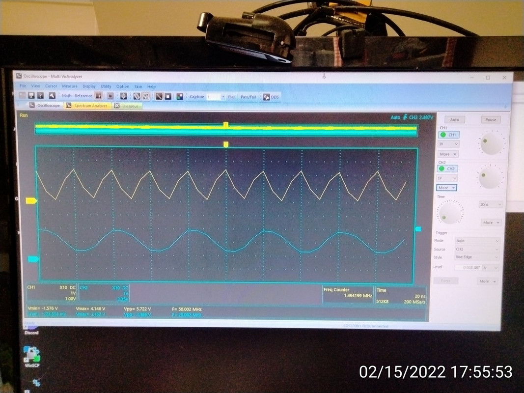
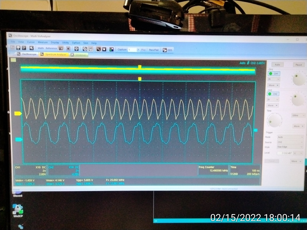
The original clock gens that are all interchangeable are: ICS9159-02, W48C60-402 (those two have both been seen), CY2254 and CGS605 (at least, according to the National Semiconductor CGS605 datasheet). It has 3 selectable Processor Clock (PClk) frequencies: 50,60 and 66MHz output on 4 pins, along with 6 Bus Clock (BClk) outputs at /2 PClk, a Floppy Controller (FDClk) clock at 24MHz, a Keyboard Controller (KBClk) clock at 12MHz and two copies of the Reference clock (REF0, REF1) at 14.318MHz.

Some hunting around found 2 clock gens with almost identical pinouts, which had more options for PClk, including 75 and 83MHz. Those are the PLL52c59-14A and the ICS5159C-14. There are two pinout differences compared to the standard chip:
1) Pin 5, the Output Enable (pull high to enable outputs) input has become the Turbo/FSel2 pin. Pulling that pin high gives the same frequency options as originally (with a bonus 55MHz in place of a test mode). Pulling it low gives 4 new frequencies, which are slightly different between the two alternate clock gens. The PLL option has 4 options for synchronous or asynchronous modes at 75 and 83Mhz. As far as I know from skimming the Intel datasheets, the chipset on the Tyan S1564 doesn't support asynchronous modes, so they're not useful in this case. The ICS option has 4 frequencies: 62,68,75 and 83MHz.

2) Pin 25, KBClk. On the original this is a 12MHz clock to the KBC. On both the alternate clock gens it's a 48MHz USB clock.

On the face of it, directly swapping them in would stop the KBC controller from working, which the BIOS would probably flag as a failed KBC. So it seemed like it would start getting messy to correct this, having to either introduce a separate KBClk, or take the USBClk and run it through a couple of flip-flops to get USBClk/4 and feed that in to the KBClk pad.

Fortunately, with a bit of following the traces, and some measurements by Sphere, we found that the Tyan has a 0 ohm link that can be used to select which clock actually drives the KBC. It can select between either pin 25 (the 12MHz part on the original clock gen, which becomes 48MHz on the alternate parts) or pin 27 (one of the 14.318MHz reference clock). It turns out that the KBC (or at least the one that Sphere tried) worked at 14.318MHz.

So if one of the alternate chips is fitted, and the 0 ohm link moved, then the board should work. That leaves just the question of how to select the extra frequencies. R48 (4.7k) pulls pin 5 high, so pin 5 can be connected directly to ground and only pull about 1mA through R48. There are several options to pull it low. Pin 4 is a ground pin, so pin 5 could just be shorted to pin 4, although that means the original frequencies can't be selected. If a jumper header is fitted between them then there will then be three jumpers, giving 8 possible frequencies. I'm not entirely happy about hooking on to a ground pin of the clock gen, so perhaps hooking on to the ground via/pin near the other frequency jumpers would be better.

Tyan_S1564D_Clock.jpg
Filename
Tyan_S1564D_Clock.jpg
File size
170.02 KiB
Views
980 views
File license
Fair use/fair dealing exception

Short version of steps:
1) Remove old clock gen
2) Fit new clock gen
3) Move 0 ohm down one place
4) Fit jumper from pin 5 to Ground.

And that should be it.

Personally, before trying this, I'd want to check the KBC was happy at 14.318. I'd keep the original clock gen in place and lift pin 25 to disconnect the KBClk pin. Then check that the BIOS halted with a failed KBC message. Then move the 0 ohm link, to connect the 14.318 reference to the KBC, and check everything to make sure the computer was stable.

Of course, all this is useless without being able to get parts. Sphere didn't have any luck with the couple of parts houses he tried. I hope this doesn't fall afoul of the no trade rules, but I did find a couple of possible sources for the ICS9159C-14. They're both AliExpress sources with very little feedback, selling used parts, so it's likely to be pot luck as to whether they are exactly the right part, not fakes, and if they actually work. But may still be worth a punt if you're feeling lucky:
https://www.aliexpress.com/item/1005002233119924.html
https://www.aliexpress.com/item/4001246130137.html

Other useful links:
CGS605 (compatible with standard clock gen) datasheet: http://pdf.datasheetcatalog.com/datasheet/nat … or/DS012491.PDF
PLL52C59-14A: http://www.ryston.cz/petr/mirror/www.phaselin … s/PDF/5914a.pdf (can be useful to search for PLL52C5914ASC, PLL52C59-14ASC)
ICS9159C-14: https://pdf.dzsc.com/9C-/ICS9159C-14_1191261.pdf (can be useful to search for ICS9159CM14, ICS9159CM-14)

Reply 43 of 105, by stamasd

User metadata
Rank l33t
Rank
l33t

https://www.ebay.com/itm/323241052254

ICS9159-c

The only issue is, I have recently had issues with this vendor on ebay. Ordered a bunch of linear voltage regulators from them, they never shipped nor answered messages.

(edit) and, oh, it's not the right IC. That one only gives 50, 60 and 66MHz only.

I/O, I/O,
It's off to disk I go,
With a bit and a byte
And a read and a write,
I/O, I/O

Reply 44 of 105, by snufkin

User metadata
Rank Oldbie
Rank
Oldbie
stamasd wrote on 2022-02-08, 21:26:

https://www.ebay.com/itm/323241052254

ICS9159-c

The only issue is, I have recently had issues with this vendor on ebay. Ordered a bunch of linear voltage regulators from them, they never shipped nor answered messages.

Mind the suffixes. The PLL one needs to be the -14A (not the -14T or the -14L) and the ICS needs to be the -14.

I think the clock manufacturers have some sort of base technology (PLL, counters, whatnot) and then they do whatever their customers want, giving each one a slightly different variant number. It's not even as though all 9159s have the same number of pins.

[edit: in fact, the -02 part on ebay is one of the original parts for the Tyan, with the 50,60,66MHz PClk options]

Reply 45 of 105, by stamasd

User metadata
Rank l33t
Rank
l33t

Okay another modern, not pin-compatible but widely available option: SI5351. It's a PLL clock generator, it has several variants but can generate simultaneously 3 to 8 different clock signals. The clock signals can be related and synced. One other problem, it works at 3.3V but line buffers/translators should take care of that. It's programmable so it should be able to generate any frequencies you want. There are also development boards available.
https://qrp-labs.com/images/synth/si5351a.pdf
https://www.amazon.com/HiLetgo-Si5351A-Freque … t/dp/B07X7ZT7KJ (not endorsing this particular vendor, just illustrating what the boards look like)

(edit) this board has on-board voltage regulator and output voltage translators already included so it can be used at 5V directly: https://www.adafruit.com/product/2045

I/O, I/O,
It's off to disk I go,
With a bit and a byte
And a read and a write,
I/O, I/O

Reply 46 of 105, by Sphere478

User metadata
Rank l33t++
Rank
l33t++

^ that looks pretty cool, I suppose we could design our own boards and buy those for the ICs and transplant
Stamasd, can you order that and try it with wires and let us know? I have some clock gens coming.

We could try both and see how it goes and decide which is best?

Sphere's PCB projects.
-
Sphere’s socket 5/7 cpu collection.
-
SUCCESSFUL K6-2+ to K6-3+ Full Cache Enable Mod
-
Tyan S1564S to S1564D single to dual processor conversion (also s1563 and s1562)

Reply 47 of 105, by snufkin

User metadata
Rank Oldbie
Rank
Oldbie

Ok, so I haven't laid anything out, but guess that the 20 pin QFN+crystal (woohoo, it has internal drive capacitors, so that's two less components)+regulator+buffers can probably fit within the 28 pin SOIC footprint (18mm x 7.5mm ish). The easier to hand solder 24 pin QSOP package (9mm x 6mm ish) would fit, but wouldn't leave much space for other components and routeing tracks out. If all the clock related components can fit in that footprint then maybe a small carrier with castellated edge connectors is possible. I was struggling to see how an overhanging PCB would practically work without harming the clock signal.

It has 8 clock outputs, of which 5 (PClk, BClk, FDClk, KBClk and Ref) are necessary, so there's a bit of flexibility depending on which pins are easiest to route out in the right order. Maybe use two outputs for Ref, then a couple of clock buffers to handle fan out for PClk and BClk (probably good for them to both go through buffers so they have the same delay).

Separately from the clock board, there might then need to be a separate small microcontroller to store different clock settings, connected to the I2C pins. And some means of loading new settings on to the clock gen. Looks like the NV storage is one-time programmable. So anything other than a default safe speed will have to be loaded over I2C once power is up, which sounds like that'd make power sequencing interesting. Maybe have the default be that outputs are disabled. That way power comes up with no clock to anything on the motherboard (except the RTC), the microcontroller (with it's own internal clock) can then load settings based on the existing motherboard jumpers on to the clock gen, then release the enables?

I've got a nagging feeling that we never confirmed what the actual supply voltage to the existing clock gen is. Sphere measured the R48 pull up, and that went to +5. But I don't actually know for sure what the Vcc to the chip is (pins 1,8,14,20,26 if anyone wants to check, worth checking them all since some chips can have separate supplies for each output). The CGS datasheet has recommended supply of 3.3, but it will work up to absolute max of 7V. So it could be 3.3V or 5V. If it's 3.3V then don't need to worry about level shifts.

[hmm, some interesting requirements to have the output voltage supplies come up before the main chip supply, in order to have the outputs in sync with each other. Maybe another job for the microcontroller, to switch a FET on to power up the clock gen once the output voltages are present]
[6 fanout clock buffer, 2.5mm x 2.5mm: https://uk.farnell.com/integrated-device-tech … =clock%20buffer ]

Reply 48 of 105, by Sphere478

User metadata
Rank l33t++
Rank
l33t++
snufkin wrote on 2022-02-08, 23:01:
Ok, so I haven't laid anything out, but guess that the 20 pin QFN+crystal (woohoo, it has internal drive capacitors, so that's t […]
Show full quote

Ok, so I haven't laid anything out, but guess that the 20 pin QFN+crystal (woohoo, it has internal drive capacitors, so that's two less components)+regulator+buffers can probably fit within the 28 pin SOIC footprint (18mm x 7.5mm ish). The easier to hand solder 24 pin QSOP package (9mm x 6mm ish) would fit, but wouldn't leave much space for other components and routeing tracks out. If all the clock related components can fit in that footprint then maybe a small carrier with castellated edge connectors is possible. I was struggling to see how an overhanging PCB would practically work without harming the clock signal.

It has 8 clock outputs, of which 5 (PClk, BClk, FDClk, KBClk and Ref) are necessary, so there's a bit of flexibility depending on which pins are easiest to route out in the right order. Maybe use two outputs for Ref, then a couple of clock buffers to handle fan out for PClk and BClk (probably good for them to both go through buffers so they have the same delay).

Separately from the clock board, there might then need to be a separate small microcontroller to store different clock settings, connected to the I2C pins. And some means of loading new settings on to the clock gen. Looks like the NV storage is one-time programmable. So anything other than a default safe speed will have to be loaded over I2C once power is up, which sounds like that'd make power sequencing interesting. Maybe have the default be that outputs are disabled. That way power comes up with no clock to anything on the motherboard (except the RTC), the microcontroller (with it's own internal clock) can then load settings based on the existing motherboard jumpers on to the clock gen, then release the enables?

I've got a nagging feeling that we never confirmed what the actual supply voltage to the existing clock gen is. Sphere measured the R48 pull up, and that went to +5. But I don't actually know for sure what the Vcc to the chip is (pins 1,8,14,20,26 if anyone wants to check, worth checking them all since some chips can have separate supplies for each output). The CGS datasheet has recommended supply of 3.3, but it will work up to absolute max of 7V. So it could be 3.3V or 5V. If it's 3.3V then don't need to worry about level shifts.

[hmm, some interesting requirements to have the output voltage supplies come up before the main chip supply, in order to have the outputs in sync with each other. Maybe another job for the microcontroller, to switch a FET on to power up the clock gen once the output voltages are present]
[6 fanout clock buffer, 2.5mm x 2.5mm: https://uk.farnell.com/integrated-device-tech … =clock%20buffer ]

Draw me a pic of whatcha want measured and I shal provide 😀

Attachments

  • image.jpg
    Filename
    image.jpg
    File size
    1.74 MiB
    Views
    935 views
    File license
    Public domain

Sphere's PCB projects.
-
Sphere’s socket 5/7 cpu collection.
-
SUCCESSFUL K6-2+ to K6-3+ Full Cache Enable Mod
-
Tyan S1564S to S1564D single to dual processor conversion (also s1563 and s1562)

Reply 49 of 105, by snufkin

User metadata
Rank Oldbie
Rank
Oldbie

It's all the power pins really. Black probe on a ground; there's a board mounting hole nearby that should be a good ground. Then with the board off, measure the resistance to each of the blue dots (pins 4,11,17,23). Should all be the same and 0 ohms (or close to, allowing for probe resistance).

Then change to voltage and with board on measure each of the red dots (pins 1,8,14,20,26). Take care, you don't want to short any pins. Also, whilst you're doing that, double check that R48 reading from before.

Attachments

Reply 50 of 105, by stamasd

User metadata
Rank l33t
Rank
l33t

I'll have a couple of the si5351 dev boards in a few days and will start playing with them. Unfortunately my oscilloscope doesn't go above 60MHz but I should still get some usable data by playing with some lower output frequencies.

it's not so easy to get some of the frequencies needed using only integer multipliers and dividers (low jitter). For instance I can get 66.6, 75, 83.3 and 95.83MHz easily. But 24MHz and 12MHz are not easy; the closest I can get are 23.94 and 11.97 respectively. I hope that's close enough. And 14.318 is impossible using integers. I got it with 25*90/(157+144/1000) 😀

I'm wondering if it weren't viable to leave the original clockgen chip in place but disconnect the pins providing Pclk and Bclk from the motherboard, and provide only those signals from the addon Si5351 chip.

I/O, I/O,
It's off to disk I go,
With a bit and a byte
And a read and a write,
I/O, I/O

Reply 51 of 105, by snufkin

User metadata
Rank Oldbie
Rank
Oldbie

Don't forget that the 14.318 is I think actually 14.318181818181818181... (did look this up once, something to do with NTSC scan rates?), which is 315/22. I might have a look at the clock builder pro software they have and see if that makes things any clearer. Or less clear.

I think that the only relationship that matters is the BClk is PClk/2, and in phase. The rest don't matter too much. The 24MHz is used by the chipset for various things, including the FDC, so if that's too far out there might be problems reading floppies. But 1/4% out sounds like it'll be ok.

[edit: huh, quite neat. It can do exactly the right outputs. You give the software the values you want, to whatever precision you want. Then it tried to work out how to use the chip's resources to get there. And complains if it can't and asks you to contact Skyworks directly, presumably so they can sell you something that can. But in this case it works (design report attached).]

Attachments

Last edited by snufkin on 2022-02-09, 17:09. Edited 1 time in total.

Reply 52 of 105, by Sphere478

User metadata
Rank l33t++
Rank
l33t++
snufkin wrote on 2022-02-09, 10:14:

It's all the power pins really. Black probe on a ground; there's a board mounting hole nearby that should be a good ground. Then with the board off, measure the resistance to each of the blue dots (pins 4,11,17,23). Should all be the same and 0 ohms (or close to, allowing for probe resistance).

Then change to voltage and with board on measure each of the red dots (pins 1,8,14,20,26). Take care, you don't want to short any pins. Also, whilst you're doing that, double check that R48 reading from before.

I measured this from ground with board off.

I measured that resistor point at 5v

Idk if I’m comfortable taking live measurements on these small pins. Can you work with this?

Attachments

  • image.jpg
    Filename
    image.jpg
    File size
    1.87 MiB
    Views
    913 views
    File license
    Public domain

Sphere's PCB projects.
-
Sphere’s socket 5/7 cpu collection.
-
SUCCESSFUL K6-2+ to K6-3+ Full Cache Enable Mod
-
Tyan S1564S to S1564D single to dual processor conversion (also s1563 and s1562)

Reply 53 of 105, by snufkin

User metadata
Rank Oldbie
Rank
Oldbie
Sphere478 wrote on 2022-02-09, 17:04:
I measured this from ground with board off. […]
Show full quote
snufkin wrote on 2022-02-09, 10:14:

It's all the power pins really. Black probe on a ground; there's a board mounting hole nearby that should be a good ground. Then with the board off, measure the resistance to each of the blue dots (pins 4,11,17,23). Should all be the same and 0 ohms (or close to, allowing for probe resistance).

Then change to voltage and with board on measure each of the red dots (pins 1,8,14,20,26). Take care, you don't want to short any pins. Also, whilst you're doing that, double check that R48 reading from before.

I measured this from ground with board off.

I measured that resistor point at 5v

Idk if I’m comfortable taking live measurements on these small pins. Can you work with this?

Ok, looks like all the grounds are grounds, so that's as expected. It also looks like all the power pins are on the same supply as they're all between 131-132 ohms. Really need to know one of them for sure though. If it makes it any easier, you can measure pin 1 by using the pad of capacitor C20 that's connected to pin 1.

Reply 54 of 105, by stamasd

User metadata
Rank l33t
Rank
l33t
snufkin wrote on 2022-02-09, 16:59:

Don't forget that the 14.318 is I think actually 14.318181818181818181... (did look this up once, something to do with NTSC scan rates?), which is 315/22. I might have a look at the clock builder pro software they have and see if that makes things any clearer. Or less clear.

I think that the only relationship that matters is the BClk is PClk/2, and in phase. The rest don't matter too much. The 24MHz is used by the chipset for various things, including the FDC, so if that's too far out there might be problems reading floppies. But 1/4% out sounds like it'll be ok.

[edit: huh, quite neat. It can do exactly the right outputs. You give the software the values you want, to whatever precision you want. Then it tried to work out how to use the chip's resources to get there. And complains if it can't and asks you to contact Skyworks directly, presumably so they can sell you something that can. But in this case it works (design report attached).]

It's actually quite easy to figure those out manually.
25*16/6=66.666
25*18/6=75
25*20/6=83.333
25*23/6=95.833
for Pclk; for Bclk you just use the same PLL on the next output and add an extra R divider of 2

12 and 24MHz I could get the easiest from the 95.833 above with extra dividers of 4 and 8.
And the 14.318 is 25*90/157.141 (instead of 157.144, this gives you more decimal places if you prefer)

or you can even make it 157 + 141359/1000000, why not. 😀

(edit) But again, I think it may be a good approach to leave the ICL9159 in place and just disconnect its Pclk and Bclk outputs from the motherboard, and supply those from the SI5351. This way, the clocks for KB, FD and ref can still be supplied from the ICL. I think this would avoid further complications and further RF taps/traces.

(more edit) Here's a quick-and-dirty Arduino sketch to set the outputs on one of the 3-output module to 66.66, 33.33 and 14.318MHz respectively:

#include <Adafruit_SI5351.h>
Adafruit_SI5351 clockgen = Adafruit_SI5351();
void setup(void)
{
Serial.begin(9600);
Serial.println("Si5351 Clockgen Test"); Serial.println("");
if (clockgen.begin() != ERROR_NONE)
{
Serial.print("Ooops, no Si5351 detected ... Check your wiring or I2C ADDR!");
while(1);
}
Serial.println("OK!");
Serial.println("Set PLL-A to 400MHz");
clockgen.setupPLLInt(SI5351_PLL_A, 16);/* 25*16=400 */
Serial.println("Set Output #0 to 66.66MHz");
clockgen.setupMultisynthInt(0, SI5351_PLL_A, SI5351_MULTISYNTH_DIV_6); /* 400/6=66.66 */
Serial.println("Set Output #1 to 33.33MHz");
clockgen.setupMultisynthInt(1, SI5351_PLL_A, SI5351_MULTISYNTH_DIV_6); /* same PLL_a settings as above so 66.66MHz */
clockgen.setupRdiv(1, SI5351_R_DIV_2); /* add an extra divider of 2 for 33.33MHz */
/* FRACTIONAL MODE --> More flexible but introduce clock jitter */
Serial.println("Set Output #2 to 14.318MHz");
clockgen.setupPLLInt(SI5351_PLL_B, 90); /*25*90=2250 */
clockgen.setupMultisynth(2, SI5351_PLL_B, 157, 141, 1000); /*2250/157.141=14.318351 */
/* Enable the clocks */
clockgen.enableOutputs(true);
}
void loop(void)
{
}

for testing I will probably use SI5351_MULTISYNTH_DIV_8 instead of SI5351_MULTISYNTH_DIV_6 to set outputs 0 and 1 to 50MHz and 25MHz, because neither of my 2 oscilloscopes goes over 60MHz.

As a practical application, since most of the pins on the Arduino will remain unused - one might attach a rotary encoder to select the FSB on-the-fly, and an OLED to display the current FSB. 😀

As for fan-out buffers/drivers, how about these?
https://www.onsemi.com/products/timing-logic- … buffers/nb3n551
https://www.onsemi.com/products/timing-logic- … buffers/nb3l553

(edit) this project has basically all that's needed: https://www.hackster.io/CesarSound/10khz-to-1 … -arduino-3a7cad
Only need to program a second output with half the frequency of the first one.

Last edited by stamasd on 2022-02-11, 14:39. Edited 1 time in total.

I/O, I/O,
It's off to disk I go,
With a bit and a byte
And a read and a write,
I/O, I/O

Reply 55 of 105, by Sphere478

User metadata
Rank l33t++
Rank
l33t++
snufkin wrote on 2022-02-09, 17:17:
Sphere478 wrote on 2022-02-09, 17:04:
I measured this from ground with board off. […]
Show full quote
snufkin wrote on 2022-02-09, 10:14:

It's all the power pins really. Black probe on a ground; there's a board mounting hole nearby that should be a good ground. Then with the board off, measure the resistance to each of the blue dots (pins 4,11,17,23). Should all be the same and 0 ohms (or close to, allowing for probe resistance).

Then change to voltage and with board on measure each of the red dots (pins 1,8,14,20,26). Take care, you don't want to short any pins. Also, whilst you're doing that, double check that R48 reading from before.

I measured this from ground with board off.

I measured that resistor point at 5v

Idk if I’m comfortable taking live measurements on these small pins. Can you work with this?

Ok, looks like all the grounds are grounds, so that's as expected. It also looks like all the power pins are on the same supply as they're all between 131-132 ohms. Really need to know one of them for sure though. If it makes it any easier, you can measure pin 1 by using the pad of capacitor C20 that's connected to pin 1.

3.3v to ground from cap pad closest to chip

Sphere's PCB projects.
-
Sphere’s socket 5/7 cpu collection.
-
SUCCESSFUL K6-2+ to K6-3+ Full Cache Enable Mod
-
Tyan S1564S to S1564D single to dual processor conversion (also s1563 and s1562)

Reply 56 of 105, by snufkin

User metadata
Rank Oldbie
Rank
Oldbie
Sphere478 wrote on 2022-02-11, 00:27:

3.3v to ground from cap pad closest to chip

That's good. Assuming that all the Vin pins are the same voltage (they've got the same resistance to ground, so I think it's likely) then I think that means level shifters aren't needed. Last thing, would you mind measuring the voltage on both sides of R48. I'm curious whether the inputs to the clock gen are 5V tolerant, or if they clamp the input to 3.3V.

Reply 57 of 105, by stamasd

User metadata
Rank l33t
Rank
l33t

So here's some testing with the SI5351 clockgen. Nothing very exciting yet, just confirmation that it actually works, that it can generate precise clocks and that 2 signals derived from the same PLL are in fact phase-synced.

The setup: Arduino and generator board. Ignore the transistor on the right, that's part of another project.
3.jpg

Waveforms at 50 and 25MHz. I had to fiddle with the settings a lot because my probes aren't exactlty high quality. Also the 50MHz is skirting on the limits of my oscilloscope, so I turned on some automatic smoothing of the curves.
4.jpg

And because of that for testing I fiddled with the code and halved the above, to 25 and 12.5MHz respectively, and turned off smoothing, so these are closer to the real waveforms.
5.jpg

I think these would be adequate to drive the PCLK and BCLK signals, probably through some buffers.

And the bad news: the 3rd output, the one I had calculated for 14.318MHz - was way off. It gave 8.256MHz instead. I probably messed up the calculations somewhere, but I'm too tired to double check now.

And on a final note: yes I know my phone camera is shit, but there isn't much I can do about that.

I/O, I/O,
It's off to disk I go,
With a bit and a byte
And a read and a write,
I/O, I/O

Reply 58 of 105, by stamasd

User metadata
Rank l33t
Rank
l33t

Look, ma! No computer! 😁

Same thing (25MHz top, 12.5MHz bottom) on my Hitachi V665. I like analog scopes better. You can see the actual waveforms much more accurately.

7.jpg

I/O, I/O,
It's off to disk I go,
With a bit and a byte
And a read and a write,
I/O, I/O

Reply 59 of 105, by Sphere478

User metadata
Rank l33t++
Rank
l33t++
stamasd wrote on 2022-02-16, 01:53:
Look, ma! No computer! :D […]
Show full quote

Look, ma! No computer! 😁

Same thing (25MHz top, 12.5MHz bottom) on my Hitachi V665. I like analog scopes better. You can see the actual waveforms much more accurately.

7.jpg

Oh my, I’m lovin this!! This may be the thing we’ve needed for many motherboards for quite a long time these retro motherboards have been limited by their clock gens for a long time.

Amazing work!! Can’t wait for more updates!!

Sphere's PCB projects.
-
Sphere’s socket 5/7 cpu collection.
-
SUCCESSFUL K6-2+ to K6-3+ Full Cache Enable Mod
-
Tyan S1564S to S1564D single to dual processor conversion (also s1563 and s1562)