r00tb33r wrote on 2022-11-03, 23:37:
Thanks for the info! I thought it would be as simple as that but wanted to confirm. The 245s are common enough chips not to skip them.
Yeah, the official name is "AT bus attachment" for a reason 😀. The IDE interface really just attaches the the hard drive to the 16-bit ISA (AT) bus.
r00tb33r wrote on 2022-11-03, 23:37:
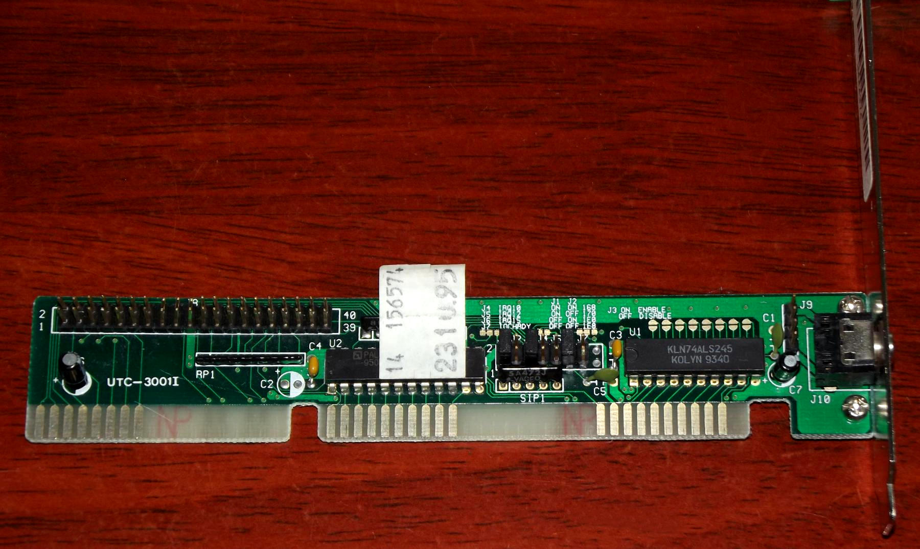
I looked up that UTC-3001I card because I was intrigued by the jack, the FCC product description says it's an audio jack? How strange! Is that just a PC speaker header?
Agreeing with jmarsh here: That card is inteded as "CD-ROM interface card" for IDE CD drives. That was at a time where analog audio playback was a relevant function of CD drives, and professional computers (opposed to gaming computers) didn't necessarily have a sound card. So they added forwarding the audio from the CD drive to allow to connect the CD audio output to a HiFi setup you already have. The audio jack is directly connected to the 4-pin header with no electronics inbetween and no connection to the ISA bus. So you could call this a "dual-function" card: It's both an IDE interface and an audio-jack carrier.
r00tb33r wrote on 2022-11-03, 23:37:
So I looked at Alexandru Groza's project, I will probably refer to it quite it bit at various times. So I looked at the schematic for that multi-IO card, and I think I see resistor network pull-ups for each IDE
interface? Those should be enabled, right? What about master/slave drives and cable select? I couldn't understand how that works.
The basic idea of the "master/slave" system is rooted in the history of IDE. Originally, the IBM AT shipped with a WD-1003 hard disc controller. That card did MFM encoding / decoding on the card itself, handled the seek pulses and head select signals, so hard drives really were just drives. This design was elegant, because it allowed two hard drives to be connected to that controller, without duplicating the controller logic. On the other hand, this design severely limited how hard drives could be designed. Most modern drives use a different number of sectors per track in different regions of the disc. The modulation scheme isn't necessarily MFM or classic RLL. Different vendors use different techniques to optimize track usage. So it turned out that it would be a smarter idea to have a controller that is more closely matched to the drive. As electronics integration density increased, there was enough space on the drive PCB to add the control logic (to integrate the drive electronics into the drive, hence the name IDE). But now we have two controllers in a two-drive setup, whereas the BIOS expects to be talking to one controller that can be told to operate on one of two drives. So the drives have to make sure that the two controllers don't interfere which each other and support all the ways the AT BIOS accesses that virtual single controller. The problem of the drives responding in a correct way that they look like a single drive is handled by the drive, not by the IDE interface card, so you just don't care about that with your card.
The pull-up/pull-down network is another funny topic: The WD-1003 interface specification states that the status register at 1F7 indicates in the top bit, whether the registers are valid at all. The idea is that the controller registers can be implemented as a single-ported 8-byte RAM chip that is assigned to be accessed by either the controller chip or the host interface. While the register set (some people call it "task file") is assigned to the controller chip, the host will read any kind of garbage, but it is guaranteed that bit 7 of 1F7 is set in this case. There are rules at what point in time the controller may claim the registers. The host needs to poll the status bit if the controller may have claimed the registers (like after you sent a command to the controller). The most important point when designing an IDE interface, though, is that the controller is default owner of the register until its power-up cycle is complete, so the BIOS has to wait till it gets access to the IDE registers before acessing the hard drive. If the BIOS tries to do auto-detection of IDE drives (i.e. something no 286 BIOS does), and there is no drive connected, it would always read 0FFh, which has its top bit set. This could mean "the drive is not ready yet" or "there is no drive". The duration after power-up until the drive is ready to respond to commands can be several tens of seconds, so a long timeout is required. This is why in IDE interface designs that are meant to be compatible with auto-probing, it is recommended to put a pull-down resistor on the IDE side of the '245 chip at D7, so if no drive responds, the host will read "7Fh" instead of "FFh". In that case, the busy bit is clear and permits the host to go on and probe whether the register set is working (which it is obviously not if there is no drive), and quickly detect if a drive is connected or not.
r00tb33r wrote on 2022-11-03, 23:37:
The image for the PAL/GAL chip is provided but sadly not source so I could look at the logic expressions. I will probably figure that out when I start working on the project. While I've been wanting to get into ATF chips (they're a superset of GALs), it's almost tempting to implement address decoding with a bunch of gates, I'm sure the combinational logic expressions are pretty simple here.
In fact the expressions are extremely simple. It's ISA, though, so be aware of a trap IBM built into the system: To avoid false decodes during DMA transfers, you must not respond to IOW or IOR while AEN is high. During DMA transfers, a memory address is on the ISA bus, a memory command line is active, and an I/O command line is active too.

 is the whole thing, and its overbuild, in reality IO cards often dispensed with 244/245 buffers