ALEKS wrote on 2024-09-05, 20:02:Well, I tested FantasyLand with the ET4000/W32i card and it doesn't work.
Here's a small clip with the display flickering around […]
Show full quote
Well, I tested FantasyLand with the ET4000/W32i card and it doesn't work.
Here's a small clip with the display flickering around: https://youtu.be/sgUEaU6eliY
I guess there's no need to fire up the Logic Analyzer anymore.
A.
Maybe it needs the translation ROM for some reason? Or is that just for CGA/MDA support?
Does the special Tseng EGA compatibility mode require the LUT translation ROM chip to work?
It's documented in the w32i manual afaik (4000AX as well documents and supports it)?
Does someone have a dump of the translation ROM btw? It'd be nice to implement that one, if possible.
Edit: So far implemented loading the 2 ROMs into UniPCemu. Also implemented the documented translation lookups, although not yet called by the CRTC and misc output register reads/writes.
Right now both ROMs are loaded seperately.
I found some clue about some people posting the ROM(s) on a forum, but it's a dead link?
https://forum.vcfed.org/index.php?threads/orc … tion-rom.57728/
Edit: Yay! Found it on minuszerodegrees!
https://www.minuszerodegrees.net/rom/rom.htm
Search for Orchid on the page for the ROM.
But that's just one 32KB ROM? Orchid is apparently an early ET4000 adaptor. And the ET4000 chip it uses uses that ROM.
Doesn't the ET4000 require 2 ROMs (as is documented) of 32KB each? Or is the ROM combined in some way?
Edit: https://dosdays.co.uk/topics/retro_review_et3000_pt1.php
OK. So a single 32KB sync ROM is correct. Then how is it wired up to the ET4000 chip (which assumes two ROM chips in it's documentation)?
How would BDB15 and DIR be wired onto this chip? Or did they only read half of the chip's contents?
Edit: Maybe it's figured out from the pins on the back and front of the images?
https://dosdays.co.uk/topics/retro_review_et3000_pt1.php
https://dosdays.co.uk/media/tsenglabs/ET3000/ … 16_et3000_1.jpg
https://dosdays.co.uk/media/tsenglabs/ET3000/ … 16_et3000_2.jpg
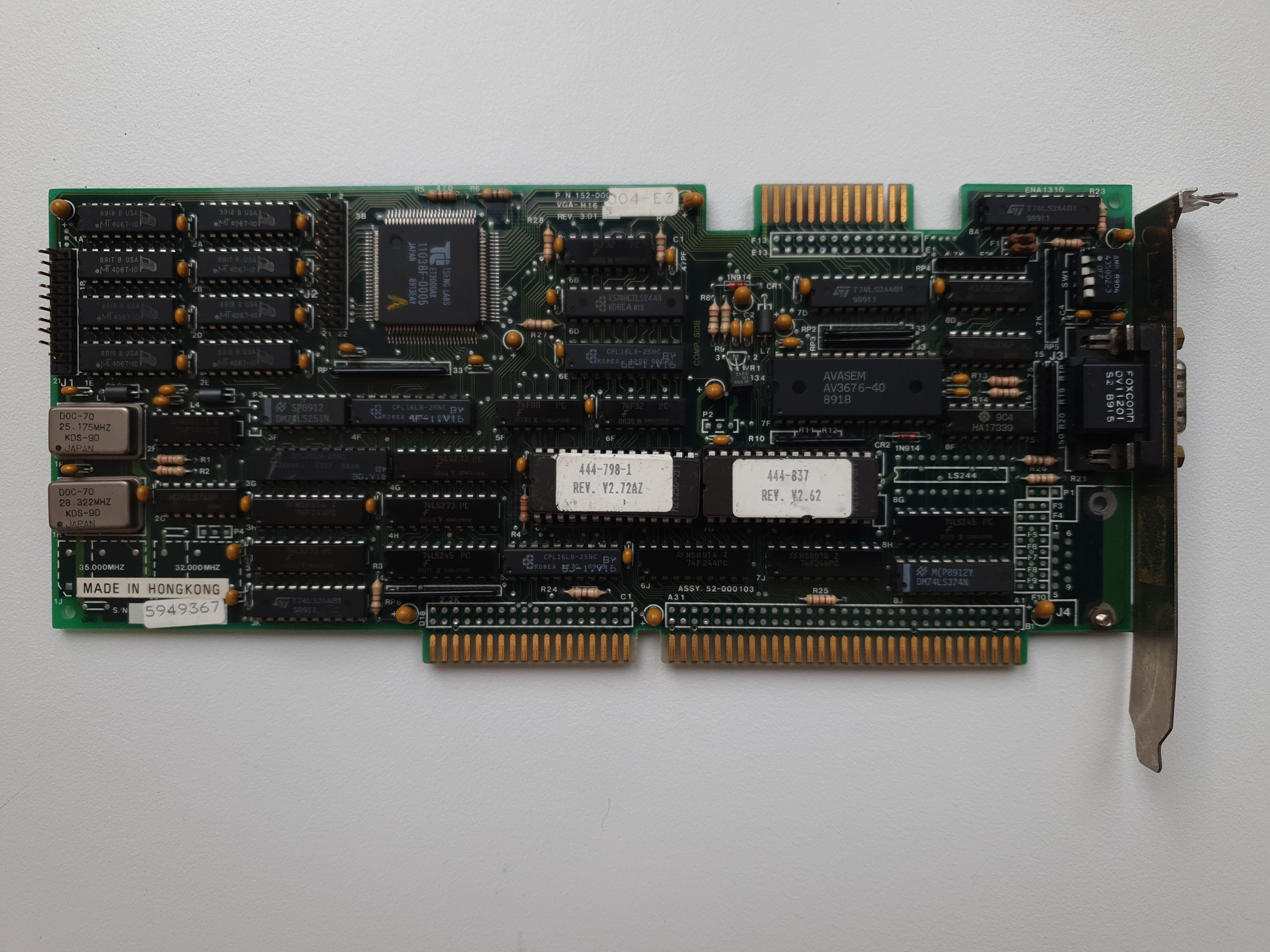
That 444.837 chip (rev. V2.62) chip seems to be the translation chip, from what's mentioned down on the page.
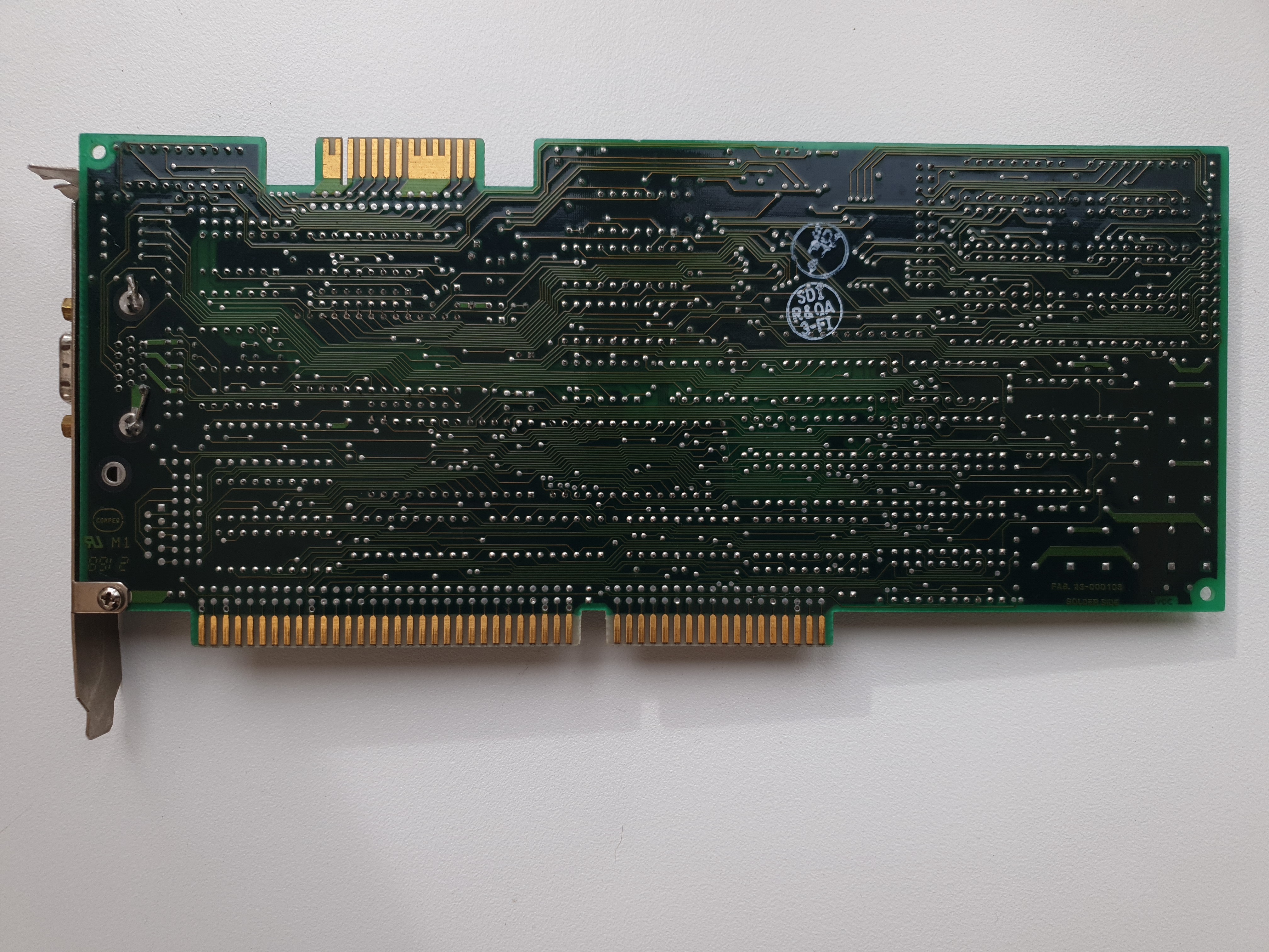
So comparing the two board photos, I at least managed to find out their locations on the backboard, I think?
The attachment ET3000_carddesign_sigma_designs_vga_h16_et3000_2_romchips.jpg is no longer available
So then it would be possible to check where those traces are going? What pins are the address (BDA) pins and DIR pin from the ET4000 connected to on the ET3000?
The ET3000AX chip faces the right side (so if turned 90 degrees clockwise it's straight?
Btw, https://thandor.net/object/529 seem to have another one on display.
Looking for the chips (https://datasheet.octopart.com/D27256-2-Intel … et-17852618.pdf) I see that the top-left pin (front) or top-right(back) is the VCC pin, followed by A14 and A13. Then A8,A9,A11,(some control line),A10,(another control line),data bus 7 through 3. The bottom row starts with A12 (opposite side of A14), then A7, A6 through A0, data line 0 through 2. The data lines give the output (which is based on the A14-A0 lines) for the reads performed from what I can see.
So now the question is how the A lines are wired to the rest of the system?
Edit: Just took a look at the ET4000 documentation again. It doesn't mention the read ROM in it's schematics?
It just mentions the write ROM in it's schematics, with BDB14-8 to A14-8(expected), DB7-0 to A7-A0(so driving the CPU input pins here), +DIR to CE(chip enable), -XROM to OE(so when a XROM lookup this is always the case, so it's always reading data from the chip! Otherwise it could mess up the data or results), BDB0-7 from Q0-Q7(the outputs of the lookup)?
For the read ROM it's apparently slightly different (seen on the Microchannel schematic, not on the AT schematic):
- BDB0-7 drive the A0-A7 inputs (the documented lookup in this case).
- DB0-7 receive the outputs from the translation.
- -DIR is used instead of +DIR. So it's not driving CE(chip enable), thus floating it's result on the AT. So during reads, the ET4000 drives it itself without translation (see explanation of RDMLL below).
Assuming XROM always properly works, this would mean that read lookups have the lower bits of the address and the output pins swap places?
So basically the write ROM translates the CPU input value in the low bits of the lookup(BDB0-7 receives the results) for CPU writes, while the read ROM translates the Tseng lookup (DB0-7(the CPU) receives the output to use by the Tseng chip(given in BDB0-7)) and gives it to the CPU directly on it's address pins? Do I understand this correctly?
The AT architecute otoh just documents the write chip, but no read chip? So the chip that's on the single-chip boards (the 32KB chips) are always write translation chips, with no read translation chips implemented?
Basically, with only 1 32KB translation chip, the chip is actually the write ROM, never the read ROM! Is that correct?
Edit: RDMLL is an interesting one in this AT configuration case. It's lowered during:
- AT VRAM reads
- AT VRAM writes
- AT BIOS reads
- AT I/O reads without translation
- AT I/O writes without translation
- Microchannel VRAM reads
- Microchannel VRAM writes
- Microchannel BIOS reads
- Microchannel I/O reads without translation
- Microchannel I/O write without translation
Lowering RDMLL causes the ET4000 to drive/receive(connect) DB0-7 itself I think (it's going through a LS245 chip from what I can read. It's inputs are -RDML(connected to OE? The documentation reads E though?) and +DIR(connected to +DIR input))? And raising RDMLL disables the outputs?
So it's not driving DB0-7 at all when it's in AT mode during any AT read/write translation at least? So when it's translating I/O reads using the translation ROM chip in AT mode, the internal DB bus is driven with the original value (which is read by the CPU even in translation mode), but since RDMLL isn't lowered, it doesn't drive the DB bus with it's value? The Microchannel one otoh doesn't use the above circuit, thus always driving DIR low and DB as is expected.
So the AT chip configuration only supports one translation chip (which is the write chip). The reads translation has no effect on the resulting data in AT mode (only in read translation ROM mode it's actually not driving the DB bits so that the result from the translation can respond)!
Edit: Just now adjusted the lookup to perform a AT-style passthough when the read translation ROM isn't loaded, otherwise use the ROM to perform proper translation (although architecturally incorrect, it eases single ROM implementations as documented).
Edit: And implemented the whole translation lookups for Misc Output register and CRTC reads/writes. It's enabled if the ENXL(writes) or ENXR(reads) are enabled, translating the values through the ROMs. And the translation function for looking up in the ROM checks for AT to disable the read translation ROM (which is currently simply based on the read translation ROM not being present).
It also has a mask and extra bits for the CGA CRTC lookup (replacing bit 4), but it's currently a if-false check since I don't know yet how the chip detects it's in 'CGA' mode for translation? The ET4000AX documentation mentions that CGA mode, but I can't find anything about how it detects that case?


