VOGONS


Reply 21 of 48, by Trashbytes

User metadata
Rank Oldbie
Rank
Oldbie
zuldan wrote on 2025-02-04, 12:30:

I’ll take the cooler off tomorrow and get some pictures…

Yeah, itll at least answer the question and give you some idea what it really is, no idea if you can still take it up with the seller.

Reply 22 of 48, by Grem Five

User metadata
Rank Member
Rank
Member
zuldan wrote on 2025-02-04, 12:18:

Here are pictures of the actual card

BF1BE4D6-7595-4657-A512-D7088A30D62C.jpeg
Filename
BF1BE4D6-7595-4657-A512-D7088A30D62C.jpeg
File size
242.84 KiB
Views
630 views
File license
Public domain
DB1E5733-B29C-4670-BF44-A0EF112097CF.jpeg
Filename
DB1E5733-B29C-4670-BF44-A0EF112097CF.jpeg
File size
711.83 KiB
Views
630 views
File license
Public domain

What made me wonder is those memory chips none of my 9800s have that style of chips, pros or XTs.

Only place I have seen that style of memory chips is here: https://archive.techarp.com/showarticle0a06.h … artno=92&pgno=2

Reply 23 of 48, by kixs

User metadata
Rank l33t
Rank
l33t
zuldan wrote on 2025-02-04, 11:03:
Ok here’s an update […]
Show full quote

Ok here’s an update

1. Disabled AGP Fast Write in the BIOS
2. Reinstalled XP
3. Installed VIA Hyperion Pro 5.24A drivers
4. Installed .NET 2.0
5. Installed Catalyst 7.11 drivers
6. Made sure V-sync was turned off
7. Set Catalyst option to Performance

Got a 3DMark03 score of 3600. A nice little improvement but still massive performance issue.

BUT…

I think I found the problem. If you look at the specs on my card

46CEEAA9-5971-4F75-B3ED-E5F9158FB6A2.jpeg
Filename
46CEEAA9-5971-4F75-B3ED-E5F9158FB6A2.jpeg
File size
107.84 KiB
Views
701 views
File license
Public domain

The graphics clock should be 412Mhz and the memory clock should be 365Mhz https://www.gpuzoo.com/GPU-ATI/Radeon_9800_XT.html

Is it possible the previous owner flashed another BIOS? Or is it possible to set the graphics and memory clock speed in the BIOS?

I really hope the previous owner hasn’t down clocked the card to hide some issue. Arrrg!!

Sometimes DDR2 memory speed is not correctly reported. As DDR2 actually doubles the clock. Not sure if this is going on here.

Visit my AmiBay items for sale:
https://www.amibay.com/members/kixs.977/#sales-threads

Reply 24 of 48, by Trashbytes

User metadata
Rank Oldbie
Rank
Oldbie
Grem Five wrote on 2025-02-04, 15:47:
zuldan wrote on 2025-02-04, 12:18:

Here are pictures of the actual card

BF1BE4D6-7595-4657-A512-D7088A30D62C.jpeg
Filename
BF1BE4D6-7595-4657-A512-D7088A30D62C.jpeg
File size
242.84 KiB
Views
630 views
File license
Public domain
DB1E5733-B29C-4670-BF44-A0EF112097CF.jpeg
Filename
DB1E5733-B29C-4670-BF44-A0EF112097CF.jpeg
File size
711.83 KiB
Views
630 views
File license
Public domain

What made me wonder is those memory chips none of my 9800s have that style of chips, pros or XTs.

Only place I have seen that style of memory chips is here: https://archive.techarp.com/showarticle0a06.h … artno=92&pgno=2

None of the 9800 cards show there even match the component layout we can see on this card, the sticker on the back suggests this is an ATI model but again it doesn't appear to follow any of the known ATI layouts for the 9800/Pro/XT. The two chokes/coils are a dead give away something isn't right here as I dont believe ATI ever used that type on their cards.

It could be a weird ATI model for all I know but too many other things are odd with it.

Could it be a modded 9800 SE ? This one from Palit uses a crazily similar board component layout along with similar ram and a 128 bit bus. This image is missing a few caps but you can see how the layout would be if they were present, the 9800SE used lower aulity parts, had similar clocks to this card but it used the R350 core.

s-l1600.jpg
Filename
s-l1600.jpg
File size
357.76 KiB
Views
345 views
File comment
Palit 9800 SE
File license
Fair use/fair dealing exception

Reply 25 of 48, by momaka

User metadata
Rank Member
Rank
Member

I'm also inclined to think this is a 9800 SE with 128-bit mem bus... but let's see.
For situations like that, it might be worth trying an older versions of GPU-Z, like v1.xx.

Better yet, it's best to see the actual hardware under the cooler.
Once the cooler is removed, also see if you can read the part number on the memory chips if they don't have heatsinks on top. The last few digits after a dash at the end of the memory chip part number are usually for the timing / clock speed - i.e. 40 or just 4 typically means 4 ns chips, which translates to a running frequency of 250 MHz (500 MHz DDR). And 33 would translate to 300 MHz (600 MHz DDR).

Reply 26 of 48, by zuldan

User metadata
Rank Oldbie
Rank
Oldbie

I ran Everest, here is the result.

IMG_7508.JPG
Filename
IMG_7508.JPG
File size
931.93 KiB
Views
270 views
File license
Public domain

Will remove the cooler and take pictures later today.

Reply 27 of 48, by Trashbytes

User metadata
Rank Oldbie
Rank
Oldbie
zuldan wrote on 2025-02-05, 00:51:

I ran Everest, here is the result.

IMG_7508.JPG
Filename
IMG_7508.JPG
File size
931.93 KiB
Views
270 views
File license
Public domain

Will remove the cooler and take pictures later today.

Memory clock is incorrect should be ~730Mhz effective, GPU clock is ~100 off.

I have been digging and neither AIBs or ATI ever made a R360 core with a 128bit bus so either the bus is being read incorrectly or the Core is being read incorrectly ...im inclined with the Core being wrong due to the Ram packages not being BGA.

Reply 28 of 48, by Grem Five

User metadata
Rank Member
Rank
Member
Trashbytes wrote on 2025-02-05, 03:12:

Memory clock is incorrect should be ~730Mhz effective, GPU clock is ~100 off.

I have been digging and neither AIBs or ATI ever made a R360 core with a 128bit bus so either the bus is being read incorrectly or the Core is being read incorrectly ...im inclined with the Core being wrong due to the Ram packages not being BGA.

Well someone must have Wierd Radeon 9800 Pro by Palit - What am I dealing with?

The layout on this card reminds me of the different layouts on the 9500 series - the early ones had their memory in an "L" shaped memory configuration this board (9700 layout board) has a 256 bit memory path compared to the "inline" memory boards that they changed over to that only had 128 bits memory path.

Reply 29 of 48, by Trashbytes

User metadata
Rank Oldbie
Rank
Oldbie
Grem Five wrote on 2025-02-05, 05:27:
Trashbytes wrote on 2025-02-05, 03:12:

Memory clock is incorrect should be ~730Mhz effective, GPU clock is ~100 off.

I have been digging and neither AIBs or ATI ever made a R360 core with a 128bit bus so either the bus is being read incorrectly or the Core is being read incorrectly ...im inclined with the Core being wrong due to the Ram packages not being BGA.

Well someone must have Wierd Radeon 9800 Pro by Palit - What am I dealing with?

The layout on this card reminds me of the different layouts on the 9500 series - the early ones had their memory in an "L" shaped memory configuration this board (9700 layout board) has a 256 bit memory path compared to the "inline" memory boards that they changed over to that only had 128 bits memory path.

They have a R350 core which is the same as used on the 9800 SE, the die picture doesn't look right, looks like a rebadged R350 .. Have seen them do this with other ATI card from back in the day.

The R350 and R360 are almost identical so its odd they would even bother.

Reply 30 of 48, by RandomStranger

User metadata
Rank Oldbie
Rank
Oldbie

Radeon 9800 series cards were a bit messy by the end of the generation. There were SE, LE and XL versions with 128bit bus, some SE did have RV360 GPUs, there were also 128bit Pro versions, like the PowerColor Radeon 9800 Pro EZ (R98-PC3F/128bit) and the Sapphire Radeon 9800 Pro Atlantis.

The Sapphire card had in-line RAM, but otherwise the component layout doesn't match:
https://pics.computerbase.de/7/7/2/5/1-1080.2986411460.jpg

Probably one of the above (RV360 128bit Pro or SE) got flashed with a modified XT BIOS. Or some Chinese frankencard maybe.

sreq.png retrogamer-s.png

Reply 31 of 48, by zuldan

User metadata
Rank Oldbie
Rank
Oldbie

Here we go, The Grand Reveal..................What are your thoughts? Any way to tell if it's Pro or SE?

Card.JPG
Filename
Card.JPG
File size
1.83 MiB
Views
192 views
File license
Public domain
GPU.JPG
Filename
GPU.JPG
File size
1.62 MiB
Views
192 views
File license
Public domain
Memory.JPG
Filename
Memory.JPG
File size
1.78 MiB
Views
192 views
File license
Public domain

Reply 32 of 48, by Trashbytes

User metadata
Rank Oldbie
Rank
Oldbie
zuldan wrote on 2025-02-05, 07:18:
Here we go, The Grand Reveal […]
Show full quote

Here we go, The Grand Reveal

GPU.JPG
Filename
GPU.JPG
File size
1.62 MiB
Views
192 views
File license
Public domain
Card.JPG
Filename
Card.JPG
File size
1.83 MiB
Views
192 views
File license
Public domain
Memory.JPG
Filename
Memory.JPG
File size
1.78 MiB
Views
192 views
File license
Public domain

Good guessing everyone! What are your thoughts?

Ewww Nanya ram .. well that explains why its so damn slow, Im still with it being a flashed 9800 SE, it could be one of the rebadged cores or one of the defective R360 cores used on cheap OEM models. ATI did that a lot so not to throw away defective cores, just disable the broken part and use it on cheaper models.

Try flashing it with a 9800SE bios and see what it does.

Reply 33 of 48, by zuldan

User metadata
Rank Oldbie
Rank
Oldbie
Trashbytes wrote on 2025-02-05, 07:21:
zuldan wrote on 2025-02-05, 07:18:
Here we go, The Grand Reveal […]
Show full quote

Here we go, The Grand Reveal

GPU.JPG
Filename
GPU.JPG
File size
1.62 MiB
Views
192 views
File license
Public domain
Card.JPG
Filename
Card.JPG
File size
1.83 MiB
Views
192 views
File license
Public domain
Memory.JPG
Filename
Memory.JPG
File size
1.78 MiB
Views
192 views
File license
Public domain

Good guessing everyone! What are your thoughts?

Ewww Nanya ram .. well that explains why its so damn slow, Im still with it being a flashed 9800 SE, it could be one of the rebadged cores or one of the defective R360 cores used on cheap OEM models. ATI did that a lot so not to throw away defective cores, just disable the broken part and use it on cheaper models.

Try flashing it with a 9800SE bios and see what it does.

I feel gutted! 🤣 I should have checked with you before purchasing the card. I'll give it a flash to a 9800 SE and see what happens.

Reply 34 of 48, by Trashbytes

User metadata
Rank Oldbie
Rank
Oldbie
zuldan wrote on 2025-02-05, 07:24:
Trashbytes wrote on 2025-02-05, 07:21:
zuldan wrote on 2025-02-05, 07:18:
Here we go, The Grand Reveal […]
Show full quote

Here we go, The Grand Reveal

GPU.JPG
Filename
GPU.JPG
File size
1.62 MiB
Views
192 views
File license
Public domain
Card.JPG
Filename
Card.JPG
File size
1.83 MiB
Views
192 views
File license
Public domain
Memory.JPG
Filename
Memory.JPG
File size
1.78 MiB
Views
192 views
File license
Public domain

Good guessing everyone! What are your thoughts?

Ewww Nanya ram .. well that explains why its so damn slow, Im still with it being a flashed 9800 SE, it could be one of the rebadged cores or one of the defective R360 cores used on cheap OEM models. ATI did that a lot so not to throw away defective cores, just disable the broken part and use it on cheaper models.

Try flashing it with a 9800SE bios and see what it does.

I feel gutted! 🤣 I should have checked with you before purchasing the card. I'll give it a flash to a 9800 SE and see what happens.

I doubt I would have been much help other than to say that's not a typical 9800 XT cooler, This type of thing happens to every one at least once so dont feel too bad.

Also dont go flashing it if you are not confident on being able to flash it back if it bricks, better to back up its BIOS first so you can at least go back.

Reply 35 of 48, by ciornyi

User metadata
Rank Member
Rank
Member

Well seems like this card is kind of aftermarket frankenstein . 5ns memory wont get anything good as its 200mhz only plus 128 bit bus .ID recommend overclock memory as fast as possible as core doesnt give you any benefit because of memory... As at other hand its unique piese of hardware aswell as late chinese geforce 6800 with 512 mb of ram which was 128 bit too

DOS: 166mmx/16mb/Y719/S3virge
DOS/95: PII333/128mb/AWE64/TNT2M64
Win98: P3 900/256mb/SB live/3dfx V3
Win Me: Athlon 1333/256mb/Audigy2/Geforce 2 GTS
Win XP: E8600/4096mb/SB X-fi/HD6850

Reply 36 of 48, by 65C02

User metadata
Rank Member
Rank
Member
zuldan wrote on 2025-02-05, 07:18:
Here we go, The Grand Reveal..................What are your thoughts? Any way to tell if it's Pro or SE? […]
Show full quote

Here we go, The Grand Reveal..................What are your thoughts? Any way to tell if it's Pro or SE?

GPU.JPG
Filename
GPU.JPG
File size
1.62 MiB
Views
192 views
File license
Public domain
Card.JPG
Filename
Card.JPG
File size
1.83 MiB
Views
192 views
File license
Public domain
Memory.JPG
Filename
Memory.JPG
File size
1.78 MiB
Views
192 views
File license
Public domain

I think that's an SE. I have the same style of card in my Athlon XP system. It is branded as a Radeon 9800SE and has the same style of memory (rectangular chips, 128 bits) and core. However mine has a Radeon 9700 type HSF and a floppy power connector. I believe it scored 4200 pts in 3DMark03.

Reply 37 of 48, by ciornyi

User metadata
Rank Member
Rank
Member
65C02 wrote on 2025-02-05, 17:57:
zuldan wrote on 2025-02-05, 07:18:
Here we go, The Grand Reveal..................What are your thoughts? Any way to tell if it's Pro or SE? […]
Show full quote

Here we go, The Grand Reveal..................What are your thoughts? Any way to tell if it's Pro or SE?

GPU.JPG
Filename
GPU.JPG
File size
1.62 MiB
Views
192 views
File license
Public domain
Card.JPG
Filename
Card.JPG
File size
1.83 MiB
Views
192 views
File license
Public domain
Memory.JPG
Filename
Memory.JPG
File size
1.78 MiB
Views
192 views
File license
Public domain

I think that's an SE. I have the same style of card in my Athlon XP system. It is branded as a Radeon 9800SE and has the same style of memory (rectangular chips, 128 bits) and core. However mine has a Radeon 9700 type HSF and a floppy power connector. I believe it scored 4200 pts in 3DMark03.

Radeon 9800 se has memory 290mhz and 3.3 ns memory chips bga or tsop . This card have 5ns chips... It is still 9800 se but cuted even worse.
Here is 9800 SE by saphire

Attachments

  • 9800SE_fhq.jpg
    Filename
    9800SE_fhq.jpg
    File size
    751.58 KiB
    Views
    114 views
    File license
    Public domain

DOS: 166mmx/16mb/Y719/S3virge
DOS/95: PII333/128mb/AWE64/TNT2M64
Win98: P3 900/256mb/SB live/3dfx V3
Win Me: Athlon 1333/256mb/Audigy2/Geforce 2 GTS
Win XP: E8600/4096mb/SB X-fi/HD6850

Reply 38 of 48, by momaka

User metadata
Rank Member
Rank
Member
zuldan wrote on 2025-02-05, 07:18:

Here we go, The Grand Reveal..................What are your thoughts? Any way to tell if it's Pro or SE?

Ooof!
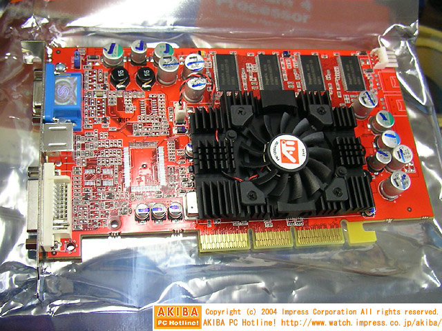
It's a SCE....... Shitty Chinese Edition.

How I know? - The dreaded Sacon FZ electrolytic capacitors, as evident by the "FZ" marks written all over them. More info on these here:
Re: Brand NEW nVidia Geforce FX5500 256MB
Basically when you see those, it's gonna be a no-name manufacturer that built the card. Only exception are some XFX cards from the GeForce 6000, 7000, and 8000 series as well as many of the early EVGA GeForce cards (I think dating as far back as the FX series.) As far as I'm aware, ATI/AMD and their AIB partners never used these crappy caps. So if you get a Radeon card with those, that's a dead giveaway it's some Chinese Frankenclone of a card.

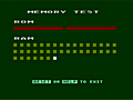
Also, as the others stated, those 5 ns memory chips are no good and your max RAM speed will likely be 200 MHz at best. If these are reject chips though, you may not even get that far... and I suspect this is why the memory frequency was turned down even lower than 200 MHz.
The core, on the other hand, should be able to OC well... but that likely won't be of any help indeed.
Now if you feel naughty and experimental, maybe try to turn down the GPU core voltage as low as possible for further reduction in heat/power consumption. With that, you could get a much longer-lasting card. Or alternatively, just use this card as-is and re-label it to remind yourself it's not an XT or PRO (or even regular non-pro) for sure.

Reply 39 of 48, by 65C02

User metadata
Rank Member
Rank
Member
ciornyi wrote on 2025-02-05, 18:33:
65C02 wrote on 2025-02-05, 17:57:
zuldan wrote on 2025-02-05, 07:18:
Here we go, The Grand Reveal..................What are your thoughts? Any way to tell if it's Pro or SE? […]
Show full quote

Here we go, The Grand Reveal..................What are your thoughts? Any way to tell if it's Pro or SE?

GPU.JPG
Filename
GPU.JPG
File size
1.62 MiB
Views
192 views
File license
Public domain
Card.JPG
Filename
Card.JPG
File size
1.83 MiB
Views
192 views
File license
Public domain
Memory.JPG
Filename
Memory.JPG
File size
1.78 MiB
Views
192 views
File license
Public domain

I think that's an SE. I have the same style of card in my Athlon XP system. It is branded as a Radeon 9800SE and has the same style of memory (rectangular chips, 128 bits) and core. However mine has a Radeon 9700 type HSF and a floppy power connector. I believe it scored 4200 pts in 3DMark03.

Radeon 9800 se has memory 290mhz and 3.3 ns memory chips bga or tsop . This card have 5ns chips... It is still 9800 se but cuted even worse.
Here is 9800 SE by saphire

That looks exactly like my card. I would have to double check the memory chips, but I'm pretty sure it's a Sapphire.