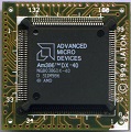
VOGONS


First post, by jakethompson1

User metadata
Rank Oldbie
Rank
Oldbie

Does anyone know if there is a backstory to how similar, yet different the UMC 85C408 is to the Genoa 6400?

The only reason this is relevant is that XFree86 supported the GVGA but not the UMC.

The ID bytes described at the very end of http://ftp.oldskool.org/pub/drivers/UMC/UM85C … .ISA/README.TXT seem deliberately designed to spoof the Genoa 6400. Tools like HWINFO then identify the card as a Genoa, but more importantly, it means the card passes the GVGA probe check in SuperProbe/XF86_SVGA.

The UM6256.DRV 640x480x256 driver for Windows 3.1 also hosted there, has a GENOA string in it.

The issue is, these two chips are not actually compatible. XFree86 produces a corrupt display. For example, both chips define port 3D4, index 06 as the bank selecting register. UMC defines the high nibble as the write bank and the low nibble as the read bank. Genoa defines bits 3-5 as the write bank, bits 0-2 as the read bank, and bit 6 to enable banking. But there are other differences including in the registers that the XF86_SVGA gvga pokes at.

More detail at https://bearstrong.net/tekst97/data/programme … ng/vgadoc3/umc/ and https://bearstrong.net/tekst97/data/programme … /vgadoc3/genoa/

Why would UMC clone a niche chip like that in an incompatible way? Or could they have been a second source for the GVGA and decided to revamp it into their own product?

Reply 1 of 13, by douglar

User metadata
Rank l33t
Rank
l33t

Perhaps they thought it was the most compatible of the day, like how Dosbox favors reporting itself as an S3 chipset?

Or perhaps a software team in UMC bought the vga bios from Genoa and didn't understand what the hardware team had done completely.

Reply 2 of 13, by mkarcher

User metadata
Rank l33t
Rank
l33t
jakethompson1 wrote on 2025-07-06, 21:15:

The issue is, these two chips are not actually compatible. XFree86 produces a corrupt display. For example, both chips define port 3D4, index 06 as the bank selecting register. UMC defines the high nibble as the write bank and the low nibble as the read bank. Genoa defines bits 3-5 as the write bank, bits 0-2 as the read bank, and bit 6 to enable banking. But there are other differences including in the registers that the XF86_SVGA gvga pokes at.

[...]

Why would UMC clone a niche chip like that in an incompatible way? Or could they have been a second source for the GVGA and decided to revamp it into their own product?

Well, you obviously notice that UMC uses 4 bits for the bank, while Genoa only uses 3 bits for the bank. The UMC 408 is not UMC's first graphics chipset, there also is the earlier 405. While 3 bits are enough to address 512K RAM at a bank size of 64K, there also is the UMC 418, a local bus chipset that supports 1M RAM, and thus needs 4 bank select bits. I think it is quite possible that the 405 is the actual Genoa 6400 clone, and the 408 is a stripped-down 418 which expanded the bank select register in an incompatible way.

Reply 3 of 13, by douglar

User metadata
Rank l33t
Rank
l33t
mkarcher wrote on 2025-07-08, 19:11:

Well, you obviously notice that UMC uses 4 bits for the bank, while Genoa only uses 3 bits for the bank. The UMC 408 is not UMC's first graphics chipset, there also is the earlier 405. While 3 bits are enough to address 512K RAM at a bank size of 64K, there also is the UMC 418, a local bus chipset that supports 1M RAM, and thus needs 4 bank select bits. I think it is quite possible that the 405 is the actual Genoa 6400 clone, and the 408 is a stripped-down 418 which expanded the bank select register in an incompatible way.

That sort of makes sense.

Any idea why my 418 would have 12 ram chips for 1.5MB ?

https://theretroweb.com/expansioncards/s/gain … d-cardex-vl-1av

Reply 4 of 13, by mkarcher

User metadata
Rank l33t
Rank
l33t
douglar wrote on 2025-07-08, 19:16:

Any idea why my 418 would have 12 ram chips for 1.5MB ?

Those UMC graphics cards never stop surprising by having very "interesting" RAM configurations. There also are a lot of 405 and 408 cards which seemingly have 768KB of RAM. For the ISA cards, I am very confident that they used factory-rejected RAM chips with damaged parts, that did no longer qualify as x4 chips, but as x3 or x2 chips. Some cards have those chips labelled A413256 (256K x 3) and A412256 (256K x 2). So each 8-bit group of the 16 bit memory is made from two x3 and one x2 chip. On those cards (nice example is the yellow one of Vlask's card at https://www.vgamuseum.info/index.php/cpu/item … -umc-um85c408af), you also have a lot of wire jumpers that actually select which data bits of the video chip are routed to which data bits of the video RAM.

I initially suspected that UMC was playing the same game again on your card, but the model number of your memory chips seem to indicate proper x4 chips, and I also don't see any configuration area on your card to choose specific bits. All UMC 418 cards I can find on VGA museum use two 256K x 16 chips, which is just 1MB, either in one bank of 32 bits, or two banks of 16 bits each. As those are VL cards, you would hope to have a 32-bit memory bus, especially as it seems the UMC 418 has a proper 32-bit VL data path (yeah, I'm looking down at you, CL-GD542x!). Your card contains 12 chips that appear to be x4 each, so this might be 3 banks of 16 bits, or one bank of 32 bits and one bank of 16 bits. Possibly 2 banks of 24 bits? Or maybe just two banks of 16 bits and they are playing the "let's use factory reject memory chips for free" game again.

I recommend you to follow traces or buzz out whether all four data pins are actually connected to the graphics chip on all of the memory chips if you want to find out what's actually happening with the video RAM on your card.

Reply 5 of 13, by jakethompson1

User metadata
Rank Oldbie
Rank
Oldbie

I did figure out modifications to XFree86 to get the UMC 408 fully working with it. Now I guess I could go back and answer the 1995 Usenet posts bewildered trying to get it work with the stock gvga driver.
Beyond having a bunch of pointless differences in the registers (and I still don't know what they mean, just ended up copying the values from what the video BIOS puts there when setting these modes from DOS, until it worked), the UM408 implements a software lock on the extended registers like many other SVGA chipsets, while the GVGA didn't.

In DOS, TOPBENCH gives an a abysmal rating for the video performance portion. My card has two out of four surface mount RAM locations populated and the empty ones say 256Kx8, so it would seem I have x8 and not x4 chips, so the problem shouldn't be an 8-bit wide video memory to host interface.

This was an interesting exercise in understanding the complications of trying to provide generic SVGA support when the user hasn't supplied a driver. I knew about later VESA BIOS Extensions that allowed it in newer OSes like Windows XP. Lacking that on these 90s SVGA cards, the complication is that even if you rely on the BIOS to get into the 256-color mode you want (thus not needing card-specific dot-clock support), you need to know how to bank-switch, and that is specific to each video chip family and part of the important performance path in the video driver. I wonder what approach Microsoft used to determine which legacy ISA SVGA cards to support first in the generic Windows 3.1 SVGA driver and then later, bundled with Windows 95. Neither the GVGA nor this UMC chip made the cut for either. I also wonder why XFree86 users having problems with Modelines didn't just go into DOS, use the video BIOS to switch to the resolution they want, then run a utility to dump the applicable settings from the VGA registers (and conversely, could tweaking the "Modeline" the VBIOS uses slightly help resolve jail bar problems and other imperfections on LCD monitors when they occur?).

Reply 6 of 13, by jakethompson1

User metadata
Rank Oldbie
Rank
Oldbie

I noticed pin B08, C09, C10 are unpopulated on my UM85C408 card, I guess that is why it is slow?

Reply 7 of 13, by mkarcher

User metadata
Rank l33t
Rank
l33t
jakethompson1 wrote on 2025-07-10, 04:09:

I noticed pin B08, C09, C10 are unpopulated on my UM85C408 card, I guess that is why it is slow?

B08 unpopulated means the card is unable to signal "zero waitstate", so all I/O and memory cycles operate at "default waitstates" or even slower (if IOCHRDY requests extra wait states). The number of "default waitstates" depends on your mainboard, and often is programmable by the BIOS, sometimes adjustable using jumpers. If you can reduce "recovery time" in setup, it might help, but possibly the "recovery time" only affects I/O cycles and not memory cycles.

You do not need C09 and C10 on an ISA card unless you intend to respond to memory cycles beyond 1MB (e.g. for linear frame buffer), or you want a slight timing advance on the memory access command. D01 (MEMCS16) is very important for performance, though, as that pin is required to be activated by the target card (the VGA in this case) if it supports 16-bit memory access.

Reply 8 of 13, by jakethompson1

User metadata
Rank Oldbie
Rank
Oldbie

I got the 418 today and can confirm that the 418 and 408 are so compatible that low-level code for the 408 works on the 418.

douglar's post here of Display Doctor: Re: UMC UM85C418F RAM - 2MB possible + desirable? suggests that the 418 does not support linear addressing.
I wonder if it has any acceleration features generally (software cursor, BitBlt, etc.) or if it is just a "dumb framebuffer."

I didn't elaborate on it, but the approach suggested at one of the links above, to distinguish the GVGA from the UM85C4x8, is to lock the extended registers, verify that toggling a bit in the bank select register doesn't "stick," then unlock the extended registers, and verify that toggling a bit in the bank select register does stick. In that case, it's the UMC and not the GVGA. That could be relevant to tools like HWINFO that want to distinguish them.

In a direct conversation, mkarcher brought up the possibility that the UM85C405AF might have been closer to GVGA-compatible, but I can't find any drivers or BIOS for that chip.

Reply 9 of 13, by rmay635703

User metadata
Rank Oldbie
Rank
Oldbie
douglar wrote on 2025-07-08, 19:16:
That sort of makes sense. […]
Show full quote
mkarcher wrote on 2025-07-08, 19:11:

Well, you obviously notice that UMC uses 4 bits for the bank, while Genoa only uses 3 bits for the bank. The UMC 408 is not UMC's first graphics chipset, there also is the earlier 405. While 3 bits are enough to address 512K RAM at a bank size of 64K, there also is the UMC 418, a local bus chipset that supports 1M RAM, and thus needs 4 bank select bits. I think it is quite possible that the 405 is the actual Genoa 6400 clone, and the 408 is a stripped-down 418 which expanded the bank select register in an incompatible way.

That sort of makes sense.

Any idea why my 418 would have 12 ram chips for 1.5MB ?

https://theretroweb.com/expansioncards/s/gain … d-cardex-vl-1av

The reason is cost but also a simple matter of color depth.

RAM Requirements for video cards is as follows (in reality)

640x480-256 300k ram
800x600-256 480k ram
1024x768 -256 768kb ram
1280x1024 -256 1.25mb ram
1600x1200 -256 1.83mb ram

As you can see 640x480 and 800x600 were VERY poor choices for memory utilization but usually aligned to the max bandwidth of the ram on early cards.
That mistake was not repeated for the high end 1024x768 which was intended to fit into common ram bank sizes evenly from its beginning on NON-IBM fixed frequency screens in the early 80’s

That said IBMs PGA 5175/1501 used a raster buffer of 320kb which closely matches the 300k video frame requirement

So Video cards with a multiple of 768k were relatively common because of the cost of ram
1.5mb and 2.25mb video cards both existed in desktop and laptop forms to support the darling resolution of 1024x768 at high color and true color.

Remember that 1024x768 was a selling point for many years as being the highest practical resolution for real work in the 90’s

The subsequent AGP standard was a case of Intel sitting on the pot too long but existed in the form that it did because it was developed assuming anemic 2mb-4mb 3d cards would be standard
during one of the memory crisis that made windows 95 a bear due to the excessive cost of ram, AGPs whole point was to improve memory throughput and make system ram available to the anemic 3d video cards that lacked enough ram.
Said problem became irrelevant when the related intel starfighter graphics released as ram was then relatively abundant and inexpensive by that time.

Reply 10 of 13, by douglar

User metadata
Rank l33t
Rank
l33t
rmay635703 wrote on Yesterday, 09:42:

So Video cards with a multiple of 768k were relatively common because of the cost of ram
1.5mb and 2.25mb video cards both existed in desktop and laptop forms to support the darling resolution of 1024x768 at high color and true color.

I can think of a couple reasons why what you describe might not be the case here with my card:
* Vesa bios extensions report 1 MB ram
* Not clear than there are not enough bits in its VGA bank switching registers to use more than 1MB
* Didn’t look to me like the umc 418 drivers support high color @ 1024 or 256 color @ 1280

Even if it did support more than 1MB ram and there is a driver that supports more than 1MB of ram, the UM70C188 dac probably isn’t fast enough to generate a useful non- interlaced signal with additional memory, which sort of makes the whole thing academic for me. I dont know of any dip28 dac chips that were faster than 85Mhz

I got to go with the theory that the 12 chips were just a way of reusing 8 1/2 defective ram chips with 4 good chips. I’ll beep out the paths this upcoming week to verify that.

I didn’t start paying attention to vga cards until 1990, but my recollection was in1990 they came as 256KB (old stuff) 512KB (cheap stuff) 1MB (Good stuff). In 1993, I remember 512KB (old stuff) 1MB frame buffers (cheap stuff) and 2d accellerators (good stuff) I don’t remember seeing VGA graphics cards with 768KB or 1.5 MB of ram at that time. I’ve seen a couple wacky high end EGA cards from the 1980’s had 786KB but they were not VGA. Looking through some old computer shopper magazines and didn’t see any 768KB or 1.5MB VGA cards. They didnt seem to be common. Do you remember the names of any graphic cards that had 768KB or 1.5 MB of ram? I’d love to do some research on them if you could point me to them.

Reply 11 of 13, by jakethompson1

User metadata
Rank Oldbie
Rank
Oldbie
douglar wrote on Yesterday, 18:05:

I didn’t start paying attention to vga cards until 1990, but my recollection was in1990 they came as 256KB (old stuff) 512KB (cheap stuff) 1MB (Good stuff). In 1993, I remember 512KB (old stuff) 1MB frame buffers (cheap stuff) and 2d accellerators (good stuff) I don’t remember seeing VGA graphics cards with 768KB or 1.5 MB of ram at that time. I’ve seen a couple wacky high end EGA cards from the 1980’s had 786KB but they were not VGA. Looking through some old computer shopper magazines and didn’t see any 768KB or 1.5MB VGA cards. They didnt seem to be common. Do you remember the names of any graphic cards that had 768KB or 1.5 MB of ram? I’d love to do some research on them if you could point me to them.

I have a copy of Building a PC for Dummies dated 1998 (and suspect I got it when it was either new or nearly so). It suggests what even then I knew was an oddity: essentially it says don't bother with 486 parts even second-hand; there's no future, but suggests that a bare bones build would be a Pentium 100 or 133 with 16MB of RAM and a 512K video card. The last doesn't belong there... did anyone even make a 512K card in PCI?

I can't say I have seen a 768K or 1536K card either. Also, the GUI acceleration features make use of off-screen memory, so the excess video RAM in lower resolutions isn't necessarily wasted.

Reply 12 of 13, by rmay635703

User metadata
Rank Oldbie
Rank
Oldbie
douglar wrote on 2025-07-08, 19:16:
That sort of makes sense. […]
Show full quote
mkarcher wrote on 2025-07-08, 19:11:

Well, you obviously notice that UMC uses 4 bits for the bank, while Genoa only uses 3 bits for the bank. The UMC 408 is not UMC's first graphics chipset, there also is the earlier 405. While 3 bits are enough to address 512K RAM at a bank size of 64K, there also is the UMC 418, a local bus chipset that supports 1M RAM, and thus needs 4 bank select bits. I think it is quite possible that the 405 is the actual Genoa 6400 clone, and the 408 is a stripped-down 418 which expanded the bank select register in an incompatible way.

That sort of makes sense.

Any idea why my 418 would have 12 ram chips for 1.5MB ?

https://theretroweb.com/expansioncards/s/gain … d-cardex-vl-1av

Several things…
http://www.amoretro.de/2012/09/trident-tvga90 … -768kb-isa.html

The original 8514 standard cards had 1mb or 1.5mb of ram, full clones would likely follow that same logic unless they opted for 2mb which was very rare at the time 8514 compatibility was common.

“The 8514 initially sold for $1290 for the adapter and $270 for the 512 KB memory expansion (equivalent to $3600 and $750, respectively, in 2024).[3] The 8514/A required a Micro Channel architecture bus at a time when ISA systems were standard.”

The attachment IMG_7051.jpeg is no longer available

See last message here

Western Digital VGA ISA video card, quick test

I had a laptop with 2.25mb of video memory and several pci cards equipt the same way.

The attachment IMG_7052.jpeg is no longer available

Reply 13 of 13, by mkarcher

User metadata
Rank l33t
Rank
l33t
rmay635703 wrote on Today, 01:30:

The comments below the photo are spot on, this card does not have 768KB of actually working memory, but it uses factory reject x4 DRAM chips that still work as x2 or x3. We've seen lots of UMC 85C405 cards on the VGA museum using the same approach. The solder jumpers JP1 to JP6 are used to map a custom selection of the 24 physically present data bits to the 16 data lines of the TVGA9000 chip. This results in 512KB only.

rmay635703 wrote on Today, 01:30:

The original 8514 standard cards had 1mb or 1.5mb of ram, full clones would likely follow that same logic unless they opted for 2mb which was very rare at the time 8514 compatibility was common.

Screenshot from ardent-tool wrote:

If your 8514 card has the memory filled on the daughtercard, it has 1.5 MB of memory and will run 256 colours, if those memory sockets are empty it has 0.5 MB and will run 16 colours at that specification.

This quote seems to be wrong. The 8514/A architecture has a 256KB x 16 base memory organization (each memory location contains 4 pixels at 4 bits/pixel), which is 512KB. The full popuplation of the daughter card increases the memory width to 32 bits (each memory location contains 4 pixels at 8 bits/pixel) by adding another 256KB x 16, so the total amount is 1MB. As there is no memory on the base card, your option to upgrade the memory is "to fill the memory sockets on the daughter card". The daughter card has 16 chips of 64k x 4 soldered (512kB) and another 16 empty sockets, so you can double the memory to 1024kB.

rmay635703 wrote on Today, 01:30:

This post confirms that some VESA driver reported 768KB of memory, likely the VESA BIOS included with that card. The amount of memory physically installed on that card is 1MB (8 chips of 256K x 4) organized as a single bank of 256K x 32 (it seems the chip can also run in a downgraded configuration at 256K x 16 with the upper four memory chips on the card being replaced by empty sockets). In contrast to the TVGA card shown in the first post, selecting 24 out of 32 bits makes no sense in this case, because the WD chip uses the full 32 bit width, and every 4th byte would be missing if only 256K x 24 (768KB) was actually used on that card.

There actually is a card that uses memory with holes: The miroCRYSTAL 24S (see the thread at Re: What VGA card did I have? starting at the post I linked, the thread does contain a photo of that card). It only has one bank of 1MB (which can be used like on any other card) and 3 more banks of 24 instead of 32 bits to contain true-color pixels. In true-color mode, all 4 banks can be used at 24 bits width. In all other modes, only the first bank is usable.

rmay635703 wrote on Today, 01:30:

I had a laptop with 2.25mb of video memory and several pci cards equipt the same way.

The attachment IMG_7052.jpeg is no longer available

Yeah, this one is correct. The ET6000 required MDRAM ("multi-bank DRAM") chips. MoSys, the only supplier of those chips, manufactured MDRAM chips with 8 banks per chip (which are used to build 2MB video cards) or 9 banks per chip (which are used to build 2.25MB video cards). Don't blindly buy an ET6000 to get a 2.25MB card, though, there are a lot of 2MB cards around as well!