Ah, one of my favorite eras in x86 computing.
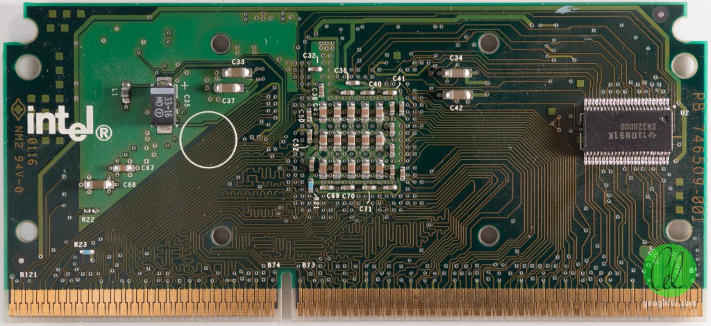
One small correction on some earlier posts, the first Slot 1 CPUs had four cache chips, not two, plus the tagRAM chip.
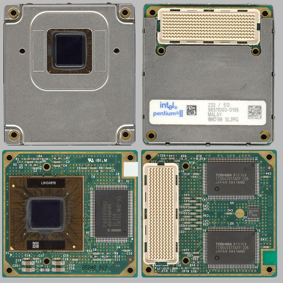
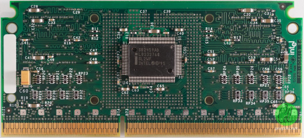
Pentium II Klamath CPU's looked like this, with the four 128K cache chips. These were only in the SECC package.

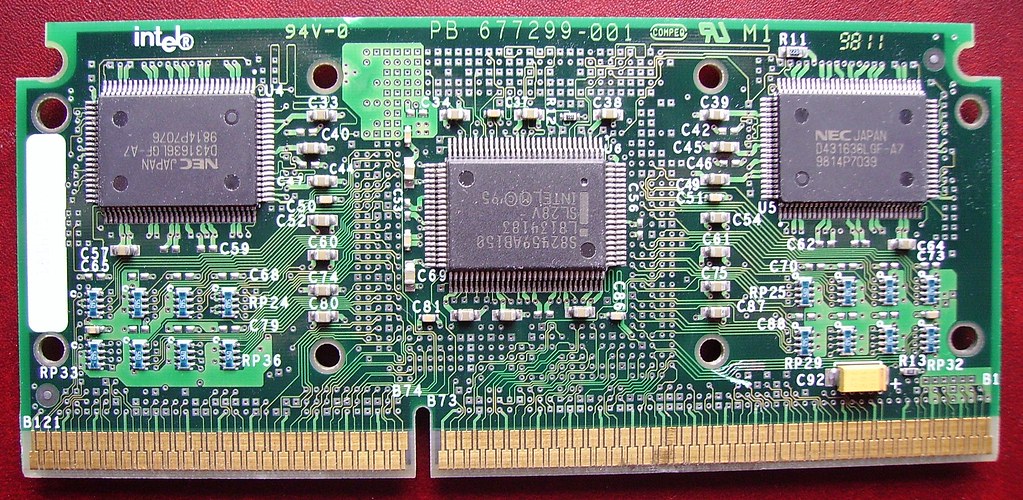
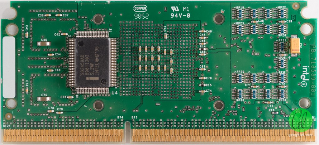
The Pentium II Deschutes CPU reduced the cache chip count down to two 256K chips. These were in SECC and SECC 2 package.
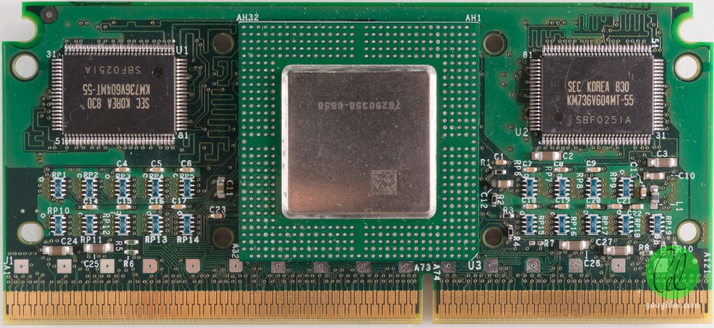
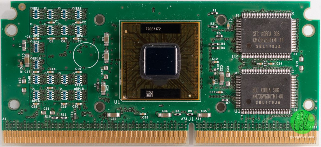
Then starting with the PII 450, and later revisions of the PII 400 and 350, we got an OLGA core and a re-arrangement of the cache chips. This same layout was also used for the PIII 450-600 Katmai CPUs. These were in SECC (only PII) and SECC 2 (PII and PIII).
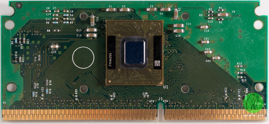
Then finally with the Coppermine core, Intel put the L2 cache on the CPU die, eliminating the need for cache chips, and leaving the Slot 1 PCB very empty. These were only in SECC 2 package.
As others have said, the Slot 1 design was a cost/performance compromise between the cheap/slow motherboard L2 cache of the Pentium and the expensive/fast full-speed L2 cache of the Pentium Pro. Over the course of 1997-1999 Intel made the move from 0.35 µm to 0.25 µm, and then 0.18 µm process technology, and as a result was able to integrate a large enough L2 cache on the CPU die at a reasonable enough cost to sell to consumers. It was also a way to force AMD off intel platforms. Once both of these objectives had been achieved, intel no longer needed the Slot 1 platform, and moved back to sockets. The Slot 1 design was a result of the state of semiconductor process technology and the positions of the key players of the industry in the mid to late-1990's.
The Celeron got on-die L2 cache even earlier than the Pentium III in the form of the famous Celeron 300A with Mendocino core. This was mostly a result of negative press on the original cache-less Celeron 266/300.