SW-SSG wrote:
...I'm pretty sure the sound chip (AY8930) and DAC on this card technically only support monophonic output, with no way for software to do arbitrary stereo panning. (Actually the AY8930 has individual outputs for each of its three voices, but I assume the original card mixes them into one and doesn't pan them around like some machines do with the AY-3-8910). If so, perhaps it's fine to go with a monophonic DAC instead, assuming such a thing exists and if it would further decrease the complexity of the PCB design/routing.
You are not 100% correct.
AY IC has three independent analog outputs: Channel A, Channel B and Channel C.
The attachment PSG.png is no longer available
Those are equal.
In some Spectrum computers those outputs were just downmixed to mono, but in others it was connected in stereo configuration.
One channel was connected to left output, another channel was connected to right output and third channel was connected to both outputs. Order (ABC) of channels was different from computer to computer, so you often could select in a software the order of channels on your exact variant.
DAC is another story... more on that later.
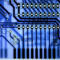
I've digged deeper into all of outputs and mixing of this board... It is a mess. I don't know what were developers of this board thinking. 😳
Analog channels A and B are indeed connected to different output channels of the soundcard. Thus you have two LM386 amplifiers onboard - it is in stereo. Channel C could be connected to both output channels. Could be, but it is not always connected. That's where weirdness starts. 😖
Analog output of Channel C from AY takes two paths.
One way is to the input of CD4066 analog switch, that is controlled from pin 7 on I/O port B of the same AY chip. Strange, but whatever. If switch is enabled then output gets mixed into both output channels via resistor mixer at same volume as Channel A and Channel B.
But there is the second way. Through the cascade on one NPN transistor it goes into... counting input of the 74HC74! 😲 Output of that D-trigger goes into 74HC125 buffer, then, if HC125 has "enable" signal, its output goes... to ISA DRQ line (DMA request)! Weirdness does not stop there. That "enable" signal for HC125 comes from pin 7 on I/O port B of AY chip, the same pin that controls switching of Channel C to analog output mixer! 🙄 A cherry on top is circuit that resets output of 74HC74 D-trigger: it is a series of NAND gates (74HC00) that sums inputs ISA_RESET and ISA_DACK (DMA acknoledgement).
So... Analog Channel C of the AY can work in two modes:
1) as normal analog output mixed as mono into output
2) as... (timed?) driver for requesting DMA from ISA bus?.. 😳
That's not everything strange in this board.
IRQ signal for ISA bus is also controlled by AY chip! The signal itself starts at GAL, that can drive Count input and Clear input of another D-trigger in 74HC74. Output of that trigger goes into another buffer in 74HC125, but before it can become ISA_IRQ signal, it must be allowed by... pin 6 on I/O port B of the AY. What the ...
And this is not finished just yet. There is one more analog switch that is controlled... You guessed it, by pin 4 on I/O port B of the AY chip. What it does? It just shunts outputs of Channel A and Channel B together (to get two channels in mono)! Screw resistor mixing and everything, just short those outputs of AY together! Why do I think that shorting two pretty low impedance outputs is a bad idea? 🙄
The attachment Untitled.png is no longer available
Well, enough of AY. Ok, it has three weirdly mixed outputs that somehow go into stereo output.
But there is one more sound source on that board, that I've mentioned earlier. That is the DAC that is formed by 74HC373 and resistor network. It is indeed, as SW-SSG was mentioning, mono. And signal from that gets buffered through emitter follower on another NPN transistor and then is mixed into both analog outputs (as mono).
There is another... well, not weirdness, but just plain error of developers of this card. 😵 Power layout. It gets power from +5V ("digital") rail, trace for it goes through the top of the board to the very left (if we look at components side) and then straight down and to ISA slot. But the return path for that current does not go to ground for those +5V. It goes for ground of +12V (that stupid ground fill at the top of the board). And that ground takes path to the very right side of the board, then straight down and into ISA slot. I'm not saying that ground of +5V is not connected with ground of +12V on the motherboard, they are. Trouble is in the path that current takes.
Did you ever heard about "loop area"? Well, as a PCB designer you always want that loop area, formed by traces for forward and return currents, to be as small as possible. That is - traces as close together as possible. For signal lines and, especially, for power rails. Now look at current path for that amplifier transistor and loop area formed by it:
The attachment bad_layout.jpg is no longer available
That loop is almost of the size of the whole board! And why that loop is bad? Because it is a loop antenna! It emits all AC that goes through those power rails into everything nearby. But antenna works both ways, so everything that is picked up by this loop will be introduced into the current that is powering that transistor. For example, all that switching noise from logic components inside the board, because:
a) every other component gets power though its own "power loop antennas", albeit smaller in size;
b) there is NONE of the bypass capacitors to smooth out those current spikes on power rails.
Just look at some examples of power routing:
The attachment bad_layout2.jpg is no longer available
I've knew that layout of this board was confusing at first glance. Now I see that there was near zero thought put into this design. Nothing to make it good quality card with clean sound.
I bet that that PCM DAC part alwayss introduces noise, hiss and other crap into output all the time. Do I have to say, that all logic ICs on the right side (74HC373, two 74HC365s and 74HC00) pull their power right through the same traces and after the AY chip? Without any decoupling. So that all dirty power on AY pins can easily be introduces into its analog outputs? 😏
I thought that SSI-2001 layout was not good... But this is just another level. A couple of them.
Oh, well. I'll make my own layout anyway, screw this original layout.
Oh, almost forgot to say.
I've got information that in one of the game that used only PCM DAC on this board it was accessed through port 0x222. So, 0x220 seems to be the default base address and port for PCM DAC is +0x02.
Also, I have to mention, that there are four resources that can be controlled:
- AY itself (with all of its registers, modes and so on)
- PCM DAC
- Joystick 1
- Joystick 2
PCM DAC can only be written and has "length" of one byte.
Each joystick can only by read and each of those also has "length" of one byte.
Almost 5 a.m. here... Seems like I have almost no time to sleep before my job. Oh, well.