feipoa wrote:If looking into making an adapter/converter, I'd start with the original MediaGX, then try for GXm, or GXi. I'd leave the AMD and more advanced chips out of it. We'd want to put the chip into a mode which bypasses the on-chip graphics, sound, and the memory controller. I've used the GXm with off-chip PCI Graphics and sound without issue.
I realize this is a pretty old post, but I'm not sure the issue was ever addressed elsewhere, though I know the topic of the pinout of the Media GX processors has come up elsewhere since:
Re: Need socket 7 Cyrix MediaGX/NS Geode pinout
same as this doccument:
http://datasheets.chipdb.org/Cyrix/MediaGX/gxmdb_v20.pdf
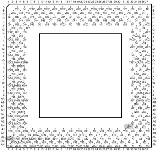
But as far as I can see from the doccumentation, there's no direct FSB/CPU bus style parallel address + data bus connection available. You get the 32-bit multiplexed address/data lines for the PCI interface (or external companion chipset interface, including PCI) and you get 64 data plus 12 multiplexed address/data lines for the local DRAM bus.
I suppose an external adapter could demultiplex the PCI bus to work on Socket 3, and maybe you could overclock that bus to 66 MHz and adjust the clock multiplier accordingly (since the Media GX core clock generator runs off the PCI frequency), but a straight passive adapter wouldn't work.
That's also why there isn't support for external L2 cache. (if it did exist it would need to be across that slow 32-bit bus ... or fudged somehow to be addressed like DRAM but without the latency)
Come to think of it, it might even be simpler to rig up external interface logic to translate the DRAM bus to a FSB for an external chipset, and you should even get a Pentium style 64-bit bus connection that way. (though things like external wait state generation might not work right since the Media GX was designed to handle all that internally and act as the bus gateway for any other chips trying to access DRAM)
That'a assuming there's not some special feature that internally remaps pins to allow a straightforward external memory interface compatible with a normal FSB, but I've never heard of anything like that. (it would've been neat and allowed Cyrix to sell Socket 3 and/or Socket 5/7 5x86/5x86MX chips using the same dies and packages as the Media GX, just with the on-chip peripheral logic disabled, sort of like AMD did with the "Athlon" variants of several of their APU lines, except all of those still retained the on-chip memory controller, but that was already standard for desktop processors by that point ... though none of those Athlon chips were AM3/3+ compatible, also not meeting the same sort of cross-platform flexibility I was thinking of)
The PGA chips already fit into normal Socket 5/7 sockets (and many Media GX/Geode boards even use stock Socket 7 ZIF sockets, confusingly ... given they still have 'Socket 7' molded into them) so it could've been a simple matter of having external jumpers/laser pits to switch the mode at the factory into a Socket 7 compatible one, but physically remapping the pins in the package would probably avoid increased on-chip complexity in the I/O section. (I don't think the physical pinout of the Media GX is very close to Socket 7 already, though given the lack of complaints of dead/exploded chips from socket mismatch, it at least sounds like they avoided reversed voltage/ground polarity and horrible short circuits, but if they'd ever intended to allow for switchable bus interface modes, the 64-bit data lines should have matched up with S5/S7 and the 32-bit PCI A/D lines probably should have matched the normal 32-bit address bus)
Mounting the BGA chips on a PGA adapter board would probably be the easier solution for all of the above (just like was already somewhat common for QFP surface mounted 386, 486, and 5x86 chips) and would've even allowed stockpiling of BGA packaged chips that later got parted out as normal desktop compatible parts. (they'd also presumably run somewhat cooler and potentially clock higher with the video and I/O functions disabled)
Socket 3 also has the larger, extended pinout with added power and ground lines normally unused by 486/5x86 processors, but might've been useful to actually implement for a higher clocked 5x86 class chip. (I forget if even the Pentium Overdrive S3 chips used those pins ... the outer pins are also the ones likely to get bent/broken, so better for those to be redundant anyway)
Given the fact Cyrix never sold Socket 3 or 7 compatible Media GX derivatives, I'm going to assume that sort of alternate bus protocol functionality isn't supported and they'd never intended it to be used as such. So stumbling on some undocumented feature that enables that would be really surprising. (I wouldn't be so surprised if there was consideration for such a feature earlier in the design and it just got dropped somewhere later on)
edit:
https://flylib.com/books/4/57/1/html/2/images/03fig18.jpg
comparing the Socket 7 pinout, there's some obvious conflict of VSS (ground) and VCC (power) lines, so plugging either chip into the wrong socket could be very bad, but I just haven't heard of many anecdotes of such or of it even killing the CPUs. (given the dramatic incident that happened with reversed polarity through an Atari VCS chipset, I'd have thought failure would be more likely ... then again I think my case coincided with the voltage regulator fusing internally and causing unregulated 9 or 12 volts reverse polarity to run through the 5V rated chips, causing dramatic popped ceramic around the dies or one or two)


