Reply 720 of 1078, by dartfrog

- Rank
- Newbie
myne wrote on 2025-04-25, 00:43:So if my understanding is correct, it is basically the same as any pci era southbridge Eg pii4x - without the extras. […]
So if my understanding is correct, it is basically the same as any pci era southbridge Eg pii4x - without the extras.
I looked at the board I extracted, and the chip itself doesn't really seem to need many supporting components.
BTW, I forgot to update the nets on the schematic.
I'll upload the one I have that is slightly updated and key components moved.
I had a quick read through some of the pii4x docs and yes seems very similar.
Thank you, that's very helpful!
RayeR wrote on 2025-04-25, 04:13:Yes, this would solve the problem if both DMA devices are on the same PCI(e) bus. But the IT8888 will be connected to different […]
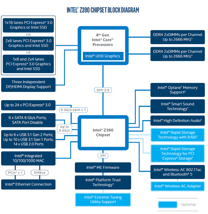
Yes, this would solve the problem if both DMA devices are on the same PCI(e) bus. But the IT8888 will be connected to different PCI bus than PCH's LPC-DMA. It depends on where the ITE will be connected, according to Z390 block diag:
https://www.guru3d.com/data/publish/200/f1ec0 … ock-diagram.png it may be attached to CPU PCIe or PCH PCIe so it depends on configuration of root PCIe bridge in CPU and PCH too. It may just happen that desired DMA IO transaction don't reach the slave PCI bus where IT8888 is waiting for bot will go to other bus with LPC block (and I guess this is the default settings as PCH still/may implements other legacy stuff like KBC, timers...), need to be checked. Maybe for some quick testing one could use some PCIe POST card: https://en.wikipedia.org/wiki/File:BIOS_POST_ … and_LPC_bus.jpg
and check if he can pass some OUT writes to port 80h at the PCIe bus supposed to connect IT8888...BTW form previous discussion I recall that intel PCH 5xx series and newer dicarded the LPC block but it still doesn't answer where legacy IO port access is routed. I don't have such new HW so can't test...
I understand now. Yeah, you're right. It absolutely matters how the motherboard implements its PCI hierarchy and where the IT8888 is attached. I would suspect that all southbridge/PCH implementations act as the sole subtractive decode agent, since there's only one subtractive decode agent allowed per PCI bus segment. This ensures that if no user device claims legacy I/O addresses, the PCH will handle them by default.
However, whether user slots are connected to that same bus or behind a PCI-PCI bridge is up to the motherboard's design. And that matters because PCI-PCI bridges typically only forward I/O transactions if the address is within their configured I/O range. From my research subtractive decode downstream of a bridge is uncommon these days, and even when possible, it still depends on whether the transaction reaches the downstream bus segment.
So realistically, the IT8888 card will only see legacy DMA I/O cycles if one of these conditions is true:
- It's on the same root PCI bus segment as the legacy I/O initiator (CPU or PCH).
- It's behind a bridge that forwards I/O cycles for the legacy DMA address ranges.
- It's behind bridge that can be configured to forward those legacy I/O ranges; which isn't always possible without BIOS or firmware support.
This IT8888 PCI/ISA card will have specific motherboard compatibility depending on it's design, and probably won't support that many boards considering how narrow the conditions I outlined above are. Even though this is all true, I will still complete the prototype and finish the PCB. There's no real reason not to. The more boards we can allow ISA, the better. I will also make the PC/PCI DMA lines easy to solder to and try to provide a non-DDMA configuration BIN so that the card can target as many boards as possible.
RayeR wrote on 2025-04-25, 04:43:UPDATE, something from PCH 6xx datasheet:
...
so legacy DMA ports are not there but as the real IO port scan could show something different...
Quickly using RWEverything on the wife's z390, only one of the five PCI-PCI bridges had I/O forwarding and not in legacy I/O ranges (IO Range 0x00003000 - 0x00003FFF). This bridge connects bus 0 to bus 1. Devices on bus 1 are behind this bridge. It's not going to work on her desktop as is. (I have a laptop so it's not worth checking).
Interesting. So basically for the maximum motherboard compatibility, you'd actually need to use a FPGA, since it's possible to emulate DMA controller registers at say some available forwarded I/O space like 0x3000–0x301F (in reference to the z390 range above). Realistically using a FPGA as a protocol converter (PCIe to ISA) and PCIe TLP modifier would be the end all be all solution, since you could largely do whatever you wanted and map it to whatever was available provided there were some forwarded I/O space the card had access to, or better yet rely on OS provided BAR resources. It's also possible you could use the IT8888 chip to handle all the ISA stuff and provide the FPGA with PCI transactions and convert the transactions into the remapped io range. Perhaps use a PCI/PCIe bridge as well to provide the FPGA with PCIe TLPs and let the FPGA only modify the TLP. Also this adds a layer so timing/latency might be an issue, so the less bridging the better. An ideal world would be FPGA implementation only. It's not magically going to support everything either. You'd still need to rewrite drivers or software to target whatever addresses too, to effectively replace the legacy path.
kagura1050 wrote on 2025-04-25, 05:46:I found a (possibly complete) schematic for a simple PCI-ISA adapter using the IT8888F on an old website of a Taiwanese prototyp […]
I found a (possibly complete) schematic for a simple PCI-ISA adapter using the IT8888F on an old website of a Taiwanese prototyping board company.
Creating a clone of this circuit might be a good starting point.https://www.costronic.com/Ev71pkit.htm
https://www.costronic.com/SH8888.pdf
Hey thanks! I mentioned costronic a page or two ago. I had no idea they had schematics. What a great find! Also the schematic clears up a confusion I had about why they wanted you to use PC/PCI DMA over DDMA, which it seems the card configuration was up to the end user so they could do either. So it's already helpful. Thanks again.
Potential PCIe-to-PCI-to-ISA pathway repository: https://github.com/DartFrogTek/PCIe-PCI-ISA
Using KMDF driver on Win10 PicoGUS PLAYS DOOM SAMPLES VIA PORT IO & DMA!