First post, by kinetix
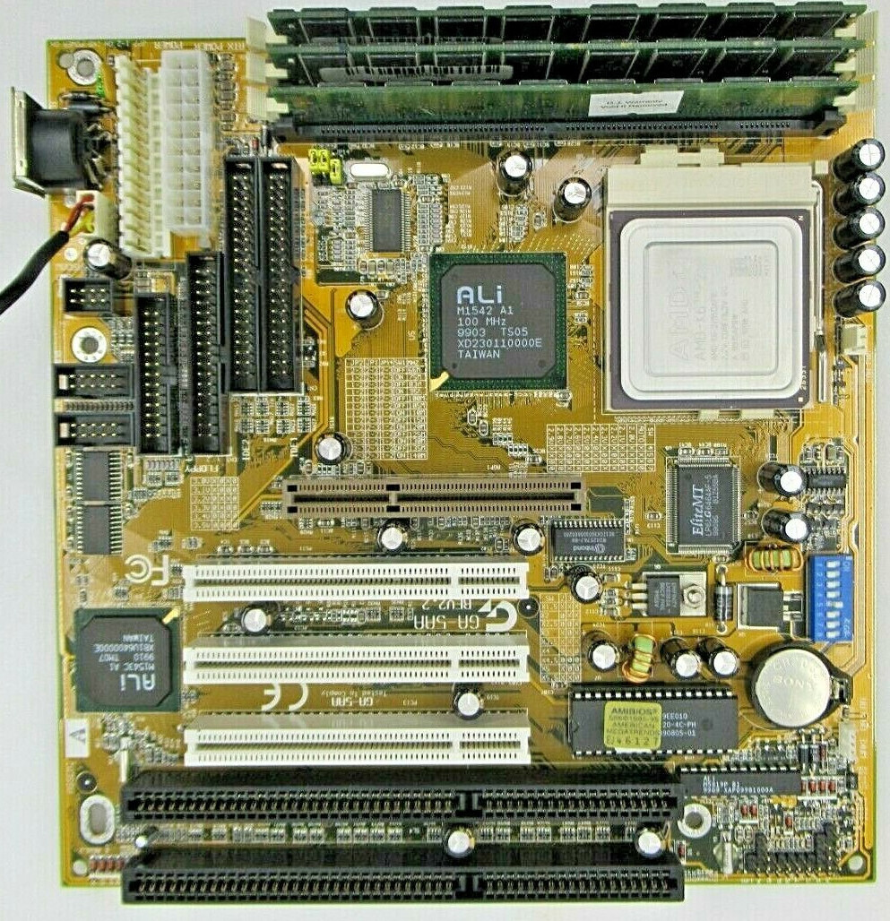
A friend gave me a nice Gigabyte GA-5AA rev 2.2 motherboard with a K6-2/450, which he had stored somewhere for many years. but it does not work. He tells me that it was functional when put away, but it kept restarting, probably due to the problem that I describe below. Hopefully with this board I can build a PC for Win98SE2 and move my PIII to Win2000 (it is the one that currently has w98se2), since I have not been able to get my other socket 7, somewhat older, to work again (nor my 486, I´m having bad luck).
Now, I need help on two topics:
1-
I have downloaded the motherboard manual. More specifically, two manuals, revision 2.2 and 3.2. Being the rev2.2 , this is the one I take as a guide. To test the board, instead of using the K6-2, as a "safety" measure I´m using a Pentium-166. BUT, the jumper/switch configuration in the manual and what is stamped on the board differ slightly!!
2-
The capacitors around the CPU, about 7, were in bad condition. This is surely the reason for the errors my friend had before on his PC.
At least the clock signals on the buses were in good shape.
I decided to change the capacitors but forgot to do one thing: to measure and photograph each welding point.
When checking the solders, now I have a position of a capacitor that gives me a "short" and that war a hard/bad soldering so I don't know what each point was like before, whether or not it had contact with which veins, and on which side.
These are later images, after desoldering the replacement capacitor to verify.
It seems to me that at the top the circular point does not make contact with the vein, but it does at the bottom (on three sides). Now, I am not sure at all about the square point in either case, it seems to me that it makes contact at the top, but at the bottom I have not been able to clean it well to see how it is (my tools leave a lot to be desired).
I found on picture of the bottom side of this board , but whoever made it had changed all those same capacitors, but left all the burned flux residue and it is impossible to see the points well.
I would appreciate if someone has one and can tell me if this "short" in that capacitor is like that. although I doubt, taking a look at the circuit. It is the TC40 capacitor.
And how are those soldering points, at least in the bottom side, were those are visible.
edit1: I found another image of the bottom side, but with worse resolution. Although I improve it with Topaz Gigapixel AI, it is not enough to be sure what the solder points are like. The round one seems like I said before, but the squared one, na-ah..


