rasz_pl wrote on 2022-12-10, 17:28:
no, and you should snip those legs flush after soldering, they do all act like mini antennas
If looks matter none, I suppose. For a compromise, I think best to snip the legs before soldering them so that solder covers the snip marks.
rasz_pl wrote on 2022-12-10, 17:28:
10 caps on the input is pure insanity :)
I think so too.
rasz_pl wrote on 2022-12-10, 17:28:
...bulk cap on the output (Cout here) helps the regulator cope with same bigger load swings
decoupling caps are near supply pins of digital logic chips to help filter out fast small spikes
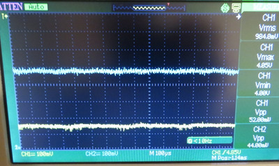
Should I check for noise on address and data pins?
Sphere478 wrote on 2022-12-10, 05:23:
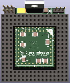
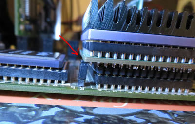
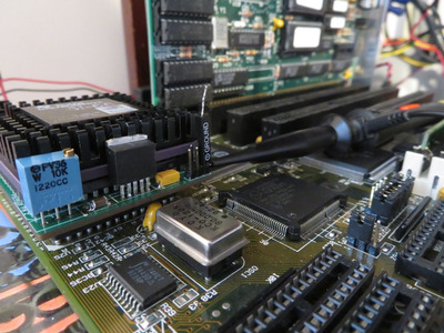
all 21 PGA caps have D shaped pads. but they are the same width as the circular pads. we can't bring them closer or it will cut the copper there.
rasz_pl wrote on 2022-12-10, 17:28:imo meh
http://axotron.se/blog/decoupling-primer/ "Impedance vs frequency plots for a few capacitors with different capacitance […]
Show full quote
imo meh
http://axotron.se/blog/decoupling-primer/ "Impedance vs frequency plots for a few capacitors with different capacitance (1 µF, 100 nF, 10 nF and 1 nF) but same size and therefore same inductance."
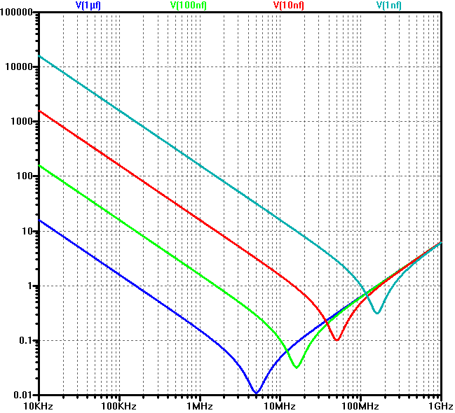
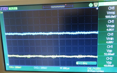
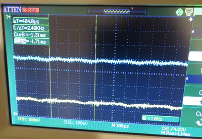
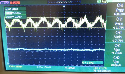
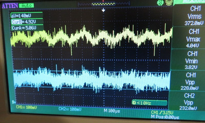
Nice and concise article with interesting plots. So if we have some noise at 40 MHz that we want to reduce, e.g. download/file.php?id=151551&mode=view , and the other values, for sake of simplicity, are in agreement with the example presented (and we omit PCB impedance) , then 1uF, 100 nF, and 10 nF all meet at the same point (40 MHz) and are already optimised, or lowest impedance, thus lowest noise?
However, the article goes on to discuss validity "up until frequencies where the plane (the PCB, I presume) starts to show its own resonances due to its distributed nature"... "The PCB layout (PCB tracks and vias) can and does add significantly to the total inductance of the capacitor."
When adding in PCB impedance (the article discusses the capacitive component in their model), I noticed the chart appears to shift considerably. So without some computer-aided modelling with the actual layout, it would be hard to know without experimentation what the theoretical best value for decoupling capacitors are. "The PCB layout (PCB tracks and vias) can and does add significantly to the total inductance of the capacitor."
Sphere478 wrote on 2022-12-10, 17:37:
This is cool. At this point we are not just making a replica unit but a superior one I think. Fingers crossed for 90mhz!
I'm pretty sure we are already running into a CPU limitation rather than a PCB limitation and any further revisions are mostly for 'making it the best it can be'. The Evergreen SXL2-66 unit might perform better because it uses a QFP package. Someone here, I think it was user Ph4nt0m, was saying that the QFP package allows for quicker heat dissipation so it has a higher probability to overclock higher. In any case, I am fairly optimistic that we can achieve 90 Mhz with peltier cooling. User pshipkov is more keen on this and has the most experience optimising the condensation factor. I already sent him some PCBs. I also have a bunch of peltiers to run this if there is sufficient interest from others. For my goals, I want heatsink/fan cooling only.
Blavius wrote on 2022-12-10, 19:44:
feipoa wrote on 2022-12-10, 05:13:
Maybe U1 and U2 will fit there as well. Only 1 person will ever use those.
Well, that person and everyone else that will put this in an IBM ;-) I didn't check the thread for a few weeks, and I'm thrilled to see the progress you guys are making. Great job on bringing the noise down and getting stable results at 80MHz. I'll try to add the same capacitors around the socket to my hacky thing, see if it makes a difference in stability.
lol, yes I know. My comment was predicting how many IBM users would use and assemble this in the next few years and I predict 1. If there are more, even better!
Plan your life wisely, you'll be dead before you know it.