snufkin wrote on 2022-02-27, 22:56:Yeah, getting a fast scope is the easiest way to tell if the clock gen is working correctly. Slowest it can be set for is 50MHz […]
Show full quote
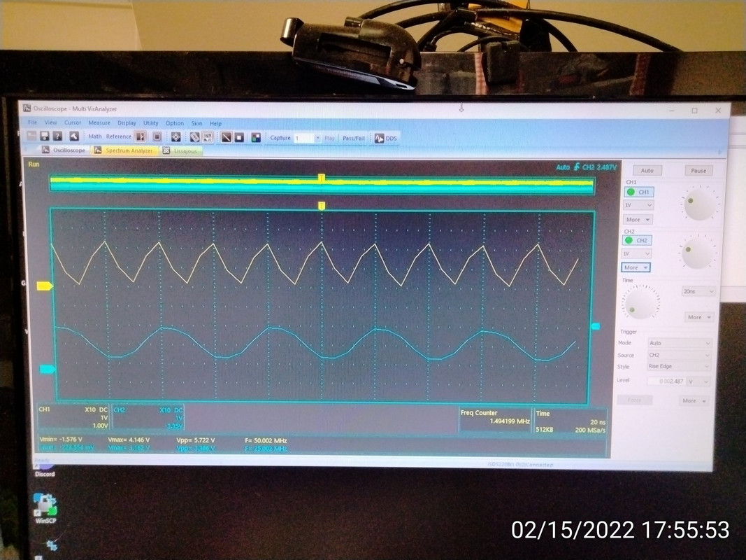
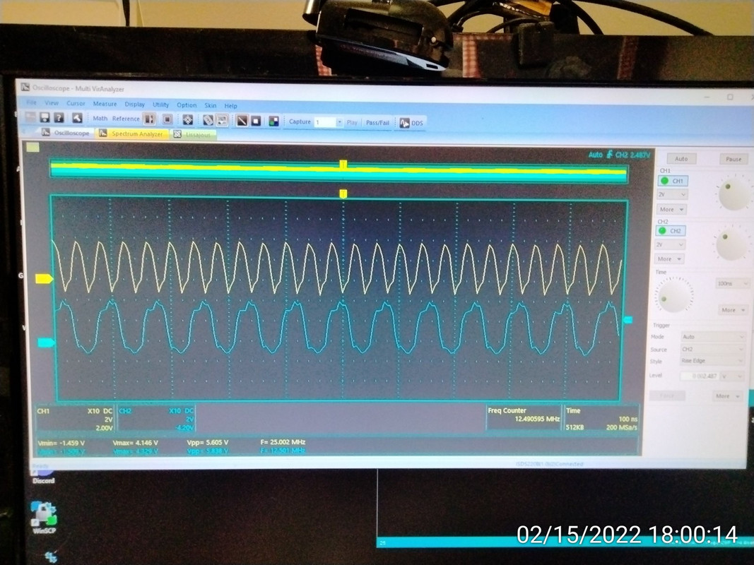
Yeah, getting a fast scope is the easiest way to tell if the clock gen is working correctly. Slowest it can be set for is 50MHz on the PClk outputs and 25MHz on the BClk.
I have had a go at tracing where all the clock outputs go:
Tyan_S1564D_Clock2.jpg
Colours are:
Blue - PClk (set by pin 5,12,13. Leave 5 disconnected and fit J13 1-2 3-4 for 50MHz).
Yellow - BClk (half frequency of PClk, in phase).
Orange - 24MHz for chipset stuff (e.g. floppy controller).
Red - 48MHz USB (this was the 12MHz KBC signal on the original one).
Green - 14.318MHz reference.
Purple - crystal drive.
I've used dotted lines to show connections through resistors. I haven't bothered to trace out the delay lines that a couple of the Bus clocks and one of the Processor clocks go through.
The only output that should be any different from the 9159-02 is the red 48MHz signal. That goes through a 22 ohm resistor, then through an empty pad, then to the original location of that 0 ohm link. Moving the 0 ohm link disconnected that and connected to the green reference clock line instead. After the 0 ohm link the trace goes up to a via between the two RAM slots, where I then loose it (top-left in the picture). But it doesn't immediately split anywhere, so there's nothing to say that it does drive more than one device.
At the moment I'd speculate that there's something up with the clockgen. Only way I can think to test that without a scope is to put the original one back (leave the 0 ohm link where it is now), then try to recreate the fault by lifting each clock output pin in turn and see if you can recreate the fault.
Okay, so you’re my brain here on this mod, 🤣 so I’m understanding that you think there is a chance the new clock gen is a:fried by r48, b: fake and I have two options: a: install another new gen, b: install the old gen to make sure the board is still okay.
I don’t see it being likely that the board is bad, so installing the old gen will probably just confirm that. And the problem is probably the 14 mhz?
I think it’s possible that the new gen is fake or damaged, so installing a new new gen is just going to confirm wether or not r48 did something, but has the chance of actually turning this into a successful mod if that is what happened.
So make a judgment call for me here. Install a new gen, or install the old gen.
I want to avoid resoldering these pads as much as possible, so if there is a way to do this with as little resolders as possible lemme know.
I don’t have a scope that will work for this unfortunately. Or access to one.
Would it be better for me to stop here and start ordering parts for that other idea?
No matter what, I don’t want to damage this board.
Your call, tell me what to do next.
Excellent work on the traces btw!! Good job!
Ultimately it seems like the other idea is a better one we can provide the exact frequencies called for to the original pins and the board should be happy? What can I do to help with the other idea?