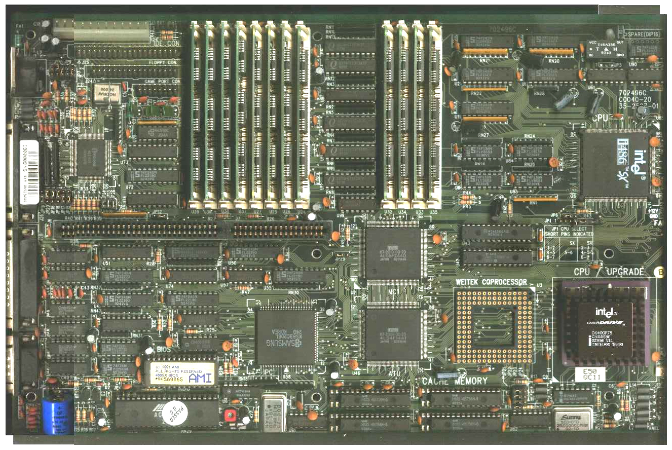
jakethompson1 wrote on 2025-04-26, 22:15:U42 (possible tag RAM) assume 62256 pinout -- 80486 address lines
A4-Vcc
A5-NC
--> Given A4 and A5, it seems an 8Kx8 SRAM actual […]
Show full quote
U42 (possible tag RAM) assume 62256 pinout -- 80486 address lines
A4-Vcc
A5-NC
--> Given A4 and A5, it seems an 8Kx8 SRAM actually belongs here?
I don't think there is an universal agreed numbering of the address pins of the 62256, but going with a common scheme, this would be pin 6 to Vcc and pin 5 not connected. Strapping pin 6 to Vcc makes sense if you want to reduce a 32K x 8 SRAM to 16K x 8, which is the usual requirement for a tag RAM at 256K cache. On the other hand, having pin 5 open makes no sense at all!. If, OTOH, you mean pin 26 is tied to Vcc and pin 1 is open, this is a correct wiring for an 8K x 8 SRAM. In that case, to make that socket compatible with 32K x 8 SRAM, apply a pull-up or pull-down (resistor or direct connection) to the unconnected pin 1.
Assuming pin 5 is open, this indicates an fault. The fault might be a missing jumper or a broken trace. Having pin 5 open causes random (likely possibly unstable) levels at that pin, that might slowly drift towards a constant 0 or 1 while the system is operating, so this is a possible cause for "works after warm-up" effects. If the open pin is pin 5, the most likely issue would be a missing jumper that toggles pin 8 between Vcc (for 8K x 8 at 128K cache) and A17 (for 256K cache).
jakethompson1 wrote on 2025-04-26, 22:15:
U43 (possible tag RAM) assume 62256 pinout -- 80486 address lines
A4-Vcc
A14--appears to go to the VTech chipset; 0.7 ohms to Vcc, 1.3 ohms to ground
0.7 ohms / 1.3 ohms doesn't make sense. I guess you mean 0.7 V / 1.3 V drop displayed in diode check mode, which would make sense for a logic level signal. Having A4 pulled to a constant level clearly seems like the board is intentionally reducing this chip from 32K x 8 to 16K x 8, which is what you would do at 256K cache. If the board supports 512K cache (using 4* 1024KBit data RAM), there should be a jumper that toggles A4 (both sockets) between Vcc and A18.
jakethompson1 wrote on 2025-04-26, 22:15:
We tried an 8Kx8 in U42 and 32Kx8 in U43 and the system locks up during POST. Various other combinations cause either a hang during POST or a false detection of 256K cache.
Assuming you used the "common" layout of 62256 pins, which has A13 and A14 on pins 1 and 26, plugging an 8K x 8 chip there would not use A4 and A5 for addressing that part of the tag, which would be bad and explain why the system doesn't work at all.
jakethompson1 wrote on 2025-04-26, 22:15:
Two traces going to the tag write enable pins looked scratched through (the blue wires are from the factory); we asked for advice at the workshop and they thought this was an intentional cut at the factory.
Yes, I agree. They bodged a "new" write-enable circuit and for that to work, they needed to disable the old write-enable circuit. Whoever installed the blue wires also cut the traces.
jakethompson1 wrote on 2025-04-26, 22:15:
It does not appear that it could be integrated comparator tag RAM because MATCH would be hardwired to Vcc. And it doesn't look like relevant x1 SRAM would be 28-pin.
Yeah, I don't think x1 SRAMs at 28 pins ever were common, so I agree with that. Integrated Comparator also looks unlikely.
jakethompson1 wrote on 2025-04-26, 22:15:
The manual says that using x9 DRAM and x8 SRAM, it is possible to have "Parity checked; must be in WT. Lower performance but better data checking." <-- this suggests there is a way to borrow data bit(s) for use as a cache parity bit instead. If both U42 & U43 are tag RAM, the tag seems unreasonably large (16 bits), looked briefly and did not look like either had obviously unused inputs.
This is an interesting clue. If you didn't mention that the 32-pin sockets were for 32K x 9, I would have expected that one of the tag RAM chips is used either as dirty (in WB mode) or as 4 parity bits (in WT mode), and it might be a x4 chip with 4 separate write enables. But possibly, both is possible: Either you install x9 SRAMs and use their dedicated parity bits, or you install x8 SRAM and repurpose the dirty tag as parity chip.
I didn't yet find x4 SRAMs with dedicated /WE inputs, but I do know that x4 DRAMs with dedicated /CAS pins to enable the individual bits do exist, and they are used on PS/2 SIMMs for parity. Given the board supports quite unusual 32K x 9 data SRAMs, I wouldn't be surprised if one of the tag chips also is a strange type. However, I did find the L7C161 and L7C162 which is an x4 chip with dedicated data in and data out, another scheme common for parity chips! This chip is claimed to be pin compatible with the IDT71981 and CY7C161 (for the L7C161) or the IDT71982 / CY7C162 (for the L7C162). On the other hand, that kind of chips doesn't have /WE on pin 27, so it likely is not the correct chip for this board, too.


