VOGONS


3 (+3 more) retro battle stations

Topic actions

Reply 1940 of 2154, by pshipkov

User metadata
Rank Oldbie
Rank
Oldbie

Agreed on long/short term usage.
For the purpose of initial inspection 1-2 weeks of grinding is a decent marker.
From there on, those who truly impress may get on a path of PC build.
That's where they meet the longer-term scrutiny with rejection being one step away at all times.

Thanks for the clarification about different OSes. Makes sense.

About different retro hardware setups - they are all neat in their own way.
I know that i am much more narrow with that stuff.

Added BIOS screens.

Your values are significantly inflated indeed. Do you remember what use cases required it ?

retro bits and bytes

Reply 1941 of 2154, by feipoa

User metadata
Rank l33t++
Rank
l33t++

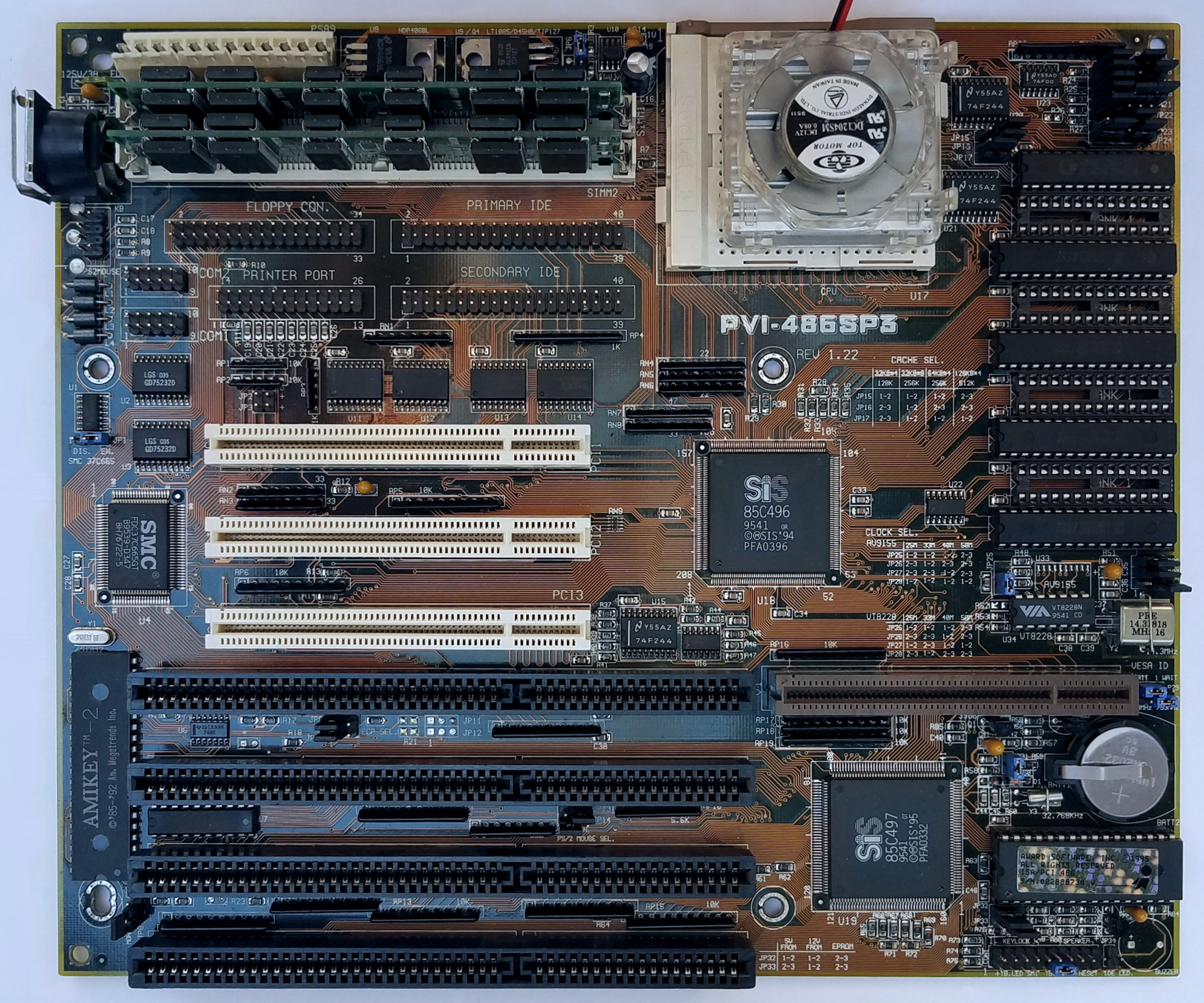
I have nearly 20 pages of hand written notes on this board over the years. With new discoveries, came more pages, thus it is really hard to follow coherently in retrospect. At first, I could only test ISA grapihcs cards, then with my skyscrapper socket stack, I could only test up to 75 MHz BL3 with VLB. With the BL3 hack, I could then start using 100 MHz, for which I employed the Promise EIDE2300plus and S3 968.

Here are some notes,

16-bit ISA 0 ws vs. 1 ws - saves 17 realtics (when using sound)
16-bit ISA Mem WS at 0 ws - saves 579 realtics (when using sound)
Delay ISA Cycle LDEVJ ws - each CLK2 saves 25-50 realtics, but only with ISA graphics

Remember to set XTOUT=0 in CTCHIP34. This saves 40 realtics.

As for the use cases requiring the reduce wait states, I do not recall. At some point, I get too bothered to keep writing reasons in the notes. It may have been related to adding two VLB cards, or to changing the sound card, or trying to get something working in NT351 for CPUID or HWINFO.

The fact that I'm running the ISA at 8.33 MHz and have reduced other 16-bit ISA properties, could imply some issue with ethernet or sound. However, it could also mean that I did not notice any substantial improvement in benchmarks, thus increased the waits for reasons of conservative. Once I moved the graphics from ISA GD5434 to VLB, the ISA speed and wait-states became less impactful on performance.

Here are some other numbers I uncovered in my notes for DOOM with BL3-100:

Trio64V+ = 26.13 fps

Trio64V+ 0ws BIOS = 26.68 fps

Trio64 w/Diamond BIOS = 26.15 fps

Trio64 w/#9 BIOS = 26.39 fps

ARK1000VL = 26.72 fps

Diamond S3 968 w/Diamond BIOS = 26.41 fps

SPEA S3 968 is a little faster than the Diamond, but I don't have the numbers written down. So either the 26.7 fps value I provided to your previously was the ARK1000VL or was the SPEA S3 968.

Plan your life wisely, you'll be dead before you know it.

Reply 1942 of 2154, by BitWrangler

User metadata
Rank l33t++
Rank
l33t++

Right ISA bus speeds can be a pain, the weak fall away at 10Mhz, even found some I/O cards don't like faster than that, usually 286 era though. Then everything gets seriously dodgy around 12Mhz or so and it's into the serious cherry picking zone. I think I had a sound and network pair getting along good at 12.5 though 3rd gen voyetra and a DE-250 IIRC.

Unicorn herding operations are proceeding, but all the totes of hens teeth and barrels of rocking horse poop give them plenty of hiding spots.

Reply 1943 of 2154, by twinge

User metadata
Rank Newbie
Rank
Newbie
pshipkov wrote on 2022-03-14, 08:03:
Alaris Cougar + BL3, 3x25, 3x33 Summary: Fastest DOS interactive graphics, fastest local storage. Slow FPU and offline compute. […]
Show full quote

Alaris Cougar + BL3, 3x25, 3x33
Summary: Fastest DOS interactive graphics, fastest local storage. Slow FPU and offline compute. Stuff just works at 3x25. Not fully stable at 3x33.
pros: 512Kb L2 cache, VLB, on-board EIDE, great assembly
cons: BL3 CPU hardcoded to 3x multiplier at start = no chance for 2x40 upon post

Few days ago I've got Alaris Cougar with BL3. Unfortunately it's impossible to switch multiplier with stock BIOS (it's locked).
So I decided to modify stock BIOS to enable software configuration option.

If someone need BIOS with disabled CRC check and disabled CPU MSR registers configuration you can download it.
With this BIOS you can use REVTO486.SYS to configure CPU.

Attachments

Reply 1944 of 2154, by pshipkov

User metadata
Rank Oldbie
Rank
Oldbie

@feipoa
I take plenty of notes to keep track of things during testing, but over time resorted to posting here a minimal version of them + the results.
Much easier to read that way. If needed, we touch on specific details in following conversations.

So, i captured the 26.7 fps in Doom properly after all.

Half a frame difference between all the cards and BIOSes.

---

@BitWrangler

Quite a few boards get way above the 10-12MHz ISA bus frequency range, with stable 27.5MHz being the peak.

---

@twinge

Congrats about the Alaris. Recently one sold for several hundred $ on ebay. Was that you on the receiving end ?
Thank you for the BIOS.

Don't use REVTO486.SYS. Use LGHT486.SYS + CTCHIP34.EXE instead to squeeze few extra bits out of the hardware.
Notice Feipoa's post above. There was in-depth conversation early in the thread and in another thread around here.
For your convenience:
In autodexe.bat put: CTCHIP34.EXE IBM486 /1000h:1:=%%1xx0xxxx
In config.sys: LGHT486.SYS /2 (or /3)

Also, linked your post from the Alaris Cougar ones early in the thread.

retro bits and bytes

Reply 1945 of 2154, by CoffeeOne

User metadata
Rank Oldbie
Rank
Oldbie
feipoa wrote on 2023-09-27, 09:18:
I'm packing my PVI board away now, but before I did, I ran some additional tests. I left graphics on VLB so that I could use CAC […]
Show full quote

I'm packing my PVI board away now, but before I did, I ran some additional tests. I left graphics on VLB so that I could use CACHE WRITE CYCLE=2. Then I tried to use a PCI network card (Realtek RTL8139D) in Win95c, but the card was undetected. If I set CACHE WRITE CYCLE back to 3, the Realtek network card worked fine. This is unfortunate because it means the issue isn't restricted to PCI graphics card.

I then put CACHE WRITE CYCLE back to 2 and was able to use a PCI Voodoo2 card just fine. So perhaps the issue with PCI and CACHE WRITE CYCLE=2 is related to assigning IRQ resources? To ensure I could still use IRQ's on other non-PCI peripherals, I connected an LPT-to-LAN ethernet adaptor. It worked fine.

So this board does have the ability to match the VLI board in raw L1/L2/DRAM speeds at 40 MHz, but with some noted caveats.

I've spent 4 nights on this board and just could not get CACHE WRITE CYCLE=2 working with PCI graphics or networking. I will be very interested to see how you were able to run your board with CACHE WRITE CYCLE set to 2 all this time.

I got some more PCI graphics cards for the the good old Asus PVI.
So my setup is still the same. 40MHz, Am5x86 @ 160MHz. Everything on max.
For now I tested only under DOS, not much time today. I ran some benchmarks and checked picture quality (on my old 19" EIZO TFT)
Biggest differences can be seen with Wolf3D, I list only this for now:

Hercules Terminator 3D / DX   110.5
Miro 40SV 102.9
ATI Graphics Pro Turbo 4MB 107.1
ATI Rage Pro PCI 4MB 111.2

The Hercules is good under DOS, picture quality OK (no jailbars), but in DOS everything was grey instead of black. A bit annoying.
Miro 40SV has very good picture quality, but is slower than all the others in DOS.
ATI Graphics Pro Turbo 4MB VRAM: Some "running jailbars" during the boot, also in 320x200 dos games. One auto reboot in a Wolf3D run, so probably not stable
ATI Rage Pro: Nice surprise: I was afraid that card might be too new for the 486 board, it is definitely not. Very good picture quality, also a tiny bit faster than the others.

I will give the ATI Rage Pro a try under windows 98SE, I believe it has a built in 250MHz RAMDAC (not sure though), which would be better than the Miro S3 968 one.
But anyway too high resolutions do not make so much sense on a 486 machine, because it kills the desktop performance.
I am quite convinced that I don't have to set cache write cycle to 3, but let's see later.

Attachments

Reply 1946 of 2154, by CoffeeOne

User metadata
Rank Oldbie
Rank
Oldbie

I started Windows 98SE with the ATI Rage Pro.

Picture quality is good, but I kept 800x600 in order to be comparable with my previous tests.
Wintune 2 800x600 16bit: 11695 (let it run 5 times and took the average). So it is still a bit slower than the optimized S3 868 VLB.
BUT: 800x600 32bit is only a tiny bit slower: 11120

So the Rage Pro for sure beats the S3 in true colour.

Machine is 100% stable, I ran this Lightwave 3d run from pshipkov.

Please also note that I did not see an IRQ assigned to the graphics card under Windows 98SE.
My previous comment about ATI Rage Pro being too new for Windows 98SE was a bit stupid. The card is from 1997, this version from Win98SE is from mid 1999.
So actually the driver installation works fully automatically, it detects the card, installs drivers. Very nice.

I attach also the BIOS settings, and a screenshot from speedsys. Interesting about the speedsys results is the relatively low harddisk speed. I use the onboard IDE controller + XT IDE Bios + Compact Flash cards Transcend 16GB.

Attachments

Reply 1947 of 2154, by CoffeeOne

User metadata
Rank Oldbie
Rank
Oldbie
pshipkov wrote on 2023-10-18, 16:27:

Was the perf improvement based on the memclock increase, or there was contribution from the 1.01 microcode ?
Can you share the 1.01 version please ?

I attached the original Elsa Bios here:
Re: Looking for S3 Vision868 BIOS (S3 DAC-equipped models)

I switched the VLI back to the Ark card, because I wanted to try the modified Bios (thread from Feipoa, Bios change was made by mkarcher as far as I know).
I can switch back to the S3 VLB 868 later and post the exact differences in the timing parameters (which can be read out and modified). What I did not try is the original Elsa Bios with the exact same parameter settings from the Diamond Bios. But as I wrote, the Elsa Bios is a bit annoying, because it sets 85Hz as a default for 640x480 and 800x600. That is not a good setting for a TFT 😁.

EDIT: It is an Elsa card, not a Spea, typo corrected.

Reply 1948 of 2154, by pshipkov

User metadata
Rank Oldbie
Rank
Oldbie

Very nice to see another person busting their PVI at max.

Thanks for the info on the ATI Rage Pro. Looks like it is a good late PCI card.

I have been watching the Ark1000VL high-resolution train. Good findings there.
I perceive the 486 VLB machines as DOS blasters. Naturally Ark1000 is the right fit for them. So, VLI+A1k=makes_sense.

retro bits and bytes

Reply 1949 of 2154, by feipoa

User metadata
Rank l33t++
Rank
l33t++

CoffeeOne: Are you willing to share an image of your full board? I see a snipet of your board here: download/file.php?id=171823&mode=view

It shows your board rev. is 1.2, and contains:

85C496 NU

Pshipkov's board, shown here https://www.petershipkov.com/temp/retro_pc_im … motherboard.jpg , is rev 1.22, yet contains:

85C496 OR 9541
85C497 OT 9541

My board is rev 1.8, yet contains:

85C496 NV 9617
85C497 NU 9616

pshipkov wrote on 2023-09-29, 15:34:

Version ID is not a fraction.
It is usually composed by major.minor numbers which are independent from each other.
Both boards are major version 1. The one here is minor version 22, yours is version 8.

It seems strange that version 1.8 contains the newer chipsets. I speculate that v1.8 was the PCB revision that they sold last because of the chipset dates. I think the major changes in this revision were to limit use of the 50 MHz FSB, which is why it is removed from the silkscreen. Thus, whatever the case may be with what the convention is for major.minor revisions, I don't think a larger minor revision number necessarily translates to the newer PCB. With also see this discrepancy with the Cyrix 5x86, that is S0R5 is newer than S1R3.

Based on an average of chipset datecoes found online for the PVI board, it looks to me as if the PCB's were released in this timeline, from oldest to newest: v1.22, v1.2, v1.8

The issue I had with needing to have the Cache Write Cycle set to 3, or otherwise half the hardware goes missing from the Device Manager, is still troubling me. I'm wondering if it has any thing to do with chipset versions, since aside from the FSB changes, I see no change to our PCB layout or components.

Pshipkov, are you still using the PVI board shown on page 1 of your thread? Or are you using a different board now?

I do have a pair of 85C496 OR, and 85C497 OT sitting in a bin from a desolder I did years ago and was wondering if I should place them onto my PVI rev 1.8 board in hopes of resolving this issue.

Plan your life wisely, you'll be dead before you know it.

Reply 1950 of 2154, by pshipkov

User metadata
Rank Oldbie
Rank
Oldbie

i remember looking at this before while trying to make sense of the assembly versions.
if you run broader search online you will notice that chipset and motherboard versions are all over the place.
there is no apparent pattern.
it can be something arbitrary like the fab(s) picking whatever chips they had on the shelf at the time of fullfilling their orders.

I dont think the BIOS microcodes implement EDO RAM support, do they ?
Can somebody with PVI SP3 and N# chips confirm ?

retro bits and bytes

Reply 1951 of 2154, by CoffeeOne

User metadata
Rank Oldbie
Rank
Oldbie
feipoa wrote on 2023-11-13, 23:09:
CoffeeOne: Are you willing to share an image of your full board? I see a snipet of your board here: download/file.php?id=171823 […]
Show full quote

CoffeeOne: Are you willing to share an image of your full board? I see a snipet of your board here: download/file.php?id=171823&mode=view

It shows your board rev. is 1.2, and contains:

85C496 NU

Pshipkov's board, shown here https://www.petershipkov.com/temp/retro_pc_im … motherboard.jpg , is rev 1.22, yet contains:

85C496 OR 9541
85C497 OT 9541

My board is rev 1.8, yet contains:

85C496 NV 9617
85C497 NU 9616

pshipkov wrote on 2023-09-29, 15:34:

Version ID is not a fraction.
It is usually composed by major.minor numbers which are independent from each other.
Both boards are major version 1. The one here is minor version 22, yours is version 8.

It seems strange that version 1.8 contains the newer chipsets. I speculate that v1.8 was the PCB revision that they sold last because of the chipset dates. I think the major changes in this revision were to limit use of the 50 MHz FSB, which is why it is removed from the silkscreen. Thus, whatever the case may be with what the convention is for major.minor revisions, I don't think a larger minor revision number necessarily translates to the newer PCB. With also see this discrepancy with the Cyrix 5x86, that is S0R5 is newer than S1R3.

Based on an average of chipset datecoes found online for the PVI board, it looks to me as if the PCB's were released in this timeline, from oldest to newest: v1.22, v1.2, v1.8

The issue I had with needing to have the Cache Write Cycle set to 3, or otherwise half the hardware goes missing from the Device Manager, is still troubling me. I'm wondering if it has any thing to do with chipset versions, since aside from the FSB changes, I see no change to our PCB layout or components.

Pshipkov, are you still using the PVI board shown on page 1 of your thread? Or are you using a different board now?

I do have a pair of 85C496 OR, and 85C497 OT sitting in a bin from a desolder I did years ago and was wondering if I should place them onto my PVI rev 1.8 board in hopes of resolving this issue.

Here is a picture

PXL_20231007_185431480.jpg
Filename
PXL_20231007_185431480.jpg
File size
1.88 MiB
Views
1014 views
File license
Fair use/fair dealing exception

Reply 1952 of 2154, by feipoa

User metadata
Rank l33t++
Rank
l33t++

CoffeeOne, thanks.

pshipkov wrote on 2023-11-14, 00:59:
i remember looking at this before while trying to make sense of the assembly versions. if you run broader search online you will […]
Show full quote

i remember looking at this before while trying to make sense of the assembly versions.
if you run broader search online you will notice that chipset and motherboard versions are all over the place.
there is no apparent pattern.
it can be something arbitrary like the fab(s) picking whatever chips they had on the shelf at the time of fullfilling their orders.

If you've seen rev. 1.2 with a 1996 chipset datecode, could you share the image resource? From the photos I rummaged thru, 1.2/1.22 largely came before rev. 1.8. Since the only official 50 MHz FSB running CPU was an problematic Intel 486DX50, I can see why a later model of the PVI motherboard would try to cover-up the 50 MHz FSB setting as they have. In late 1995, it would not make since to first produce a motherboard without a 50 MHz FSB, then some months later, try to add a 50 Mhz setting. People using a DX50 were usually trying to use it on a late ISA-only board, or at the latest, ISA-VLB. Not a PCI board.

To help clear this up, could you (pshipkov & CoffeeOne) read me the datecode on the bottom of your PCB? It is on the bottom of the motherboard, very close to the BIOS chip vias.

My rev. 1.8 board shows 96 10.

However, the obfuscation of the 50 MHz FSB setting still does not explain the discrepency in our results for my case of the Cache Write Cycle needing to be set to 3, or half the hardware disappears from the Dev. Mgr. I noticed that both your boards have different chipset revisons than mine, so that is what I was thinking to swap. Alternately, rev 1.2/1.22 may have slightly different values for resistors or other components. On the UUD board, I did notice that different versions had different values for a resistor used for impedence matching, specifically at the position for the CLK signal after the line driver.

pshipkov wrote on 2023-11-14, 00:59:

I dont think the BIOS microcodes implement EDO RAM support, do they ?
Can somebody with PVI SP3 and N# chips confirm ?

I think 85C496 PR is needed for EDO. I don't have any spare PR Northbridges. I'd be surprised if the BIOS had timings available for EDO memory, but its possible the firmware engineer added it as an overengineering step, like to prevent having to add it later on.

Plan your life wisely, you'll be dead before you know it.

Reply 1953 of 2154, by pshipkov

User metadata
Rank Oldbie
Rank
Oldbie

Ah, right PR, not N#.

revision 1.21 with chipset date 96 36 (this is the latest i have seen to date)
https://forum.maxiol.com/index.php?s=40b28c41 … pe=post&id=7646

I don't see any numbers on the back nearby the BIOS location on the two boards here.

Btw, what you mean with obfuscation of 50MHz ?
The jumper configuration is printed on the silkscreen.

I think i mentioned it before that i remember hitting the Cache Write Cycle = 3 issue at some point, but cannot remember under what circumstances anymore.

retro bits and bytes

Reply 1954 of 2154, by feipoa

User metadata
Rank l33t++
Rank
l33t++
pshipkov wrote on 2023-11-15, 06:58:
Ah, right PR, not N#. […]
Show full quote

Ah, right PR, not N#.

revision 1.21 with chipset date 96 36 (this is the latest i have seen to date)
https://forum.maxiol.com/index.php?s=40b28c41 … pe=post&id=7646

I don't see any numbers on the back nearby the BIOS location on the two boards here.

Btw, what you mean with obfuscation of 50MHz ?
The jumper configuration is printed on the silkscreen.

I think i mentioned it before that i remember hitting the Cache Write Cycle = 3 issue at some point, but cannot remember under what circumstances anymore.

I've never seen a v1.21 before, but does the northbridge on that board look like it was repalced, perhaps because it came with a really old variant of the SiS chipset? In this thread, user shock__ said he was intending to replace his chipsets on this very PVI board because they were older revisions. Asus PVI-486SP3 // PCB vs. Chipset Revisions

Here's another rev 1.22 with an even older Northbridge datecode of 9524: https://www.amibay.com/attachments/3-jpg.1592213/

From my experience with M919 and UUD boards, the PCB revisions loosely follow a trend of increasing IC datecodes. Looking at all the other IC's on my rev 1.8 and they all have 1996 datecodes (VRMs, Super I/O, PLL, 7400 series IC's, BIOS EEPROM), while your board's IC's are 1995.

However, it's really hard to say what is going on with these PVI revisions. It is possible that the v1.22 are the later versions, but only because Asus insisted that htey contain the OR/OT chipsets, which at the time, could be in short supply on later datecodes. To assist in this investigation, it would be helpful to see the PCB datecodes. Mine is as follows:

PVI_PCB_datecode.JPG
Filename
PVI_PCB_datecode.JPG
File size
197.86 KiB
Views
955 views
File license
CC-BY-4.0

Depending on which orientation you view the datecode, it could read either 9610, or 0196. I'd assume the orientation of the datecode would correspond to that of the YANG AN YA-1 markings, so I say it is 9610.

The obfuscation of the 50 MHz FSB setting may only refer to rev 1.8 because this is the revision which has the silkscreen removed for the 50 MHz FSB setting. To ensure that the user still could not set 50 MHz using the jumper settings from the manual, they have flipped the jumper settings for 50 MHz on rev 1.8. More on that was posted here: Re: Asus PVI-486SP3 v.1.22 and 66MHz FSB

So Asus really did not want people using 50 MHz on rev. 1.8, which makes the most sense to me if rev 1.8 was sold revision of this motherboard. I suspect the revisions printed for this board may be a decimal fraction.

Do you recall which BIOS version came on your PVI board? This could shed some light as well. I think mine originally had v305 or v306.

Plan your life wisely, you'll be dead before you know it.

Reply 1955 of 2154, by pshipkov

User metadata
Rank Oldbie
Rank
Oldbie

The soldered pins look too regular for the home hack jobs we do, but who knows. It is possible.

oh, wow. I actually participated in the thread you linked first.
Notice the chipset revision list i provided.
Now it is coming back to me.
OR/OT is the latest stepping.
All 1.22 revisions are with that stepping.
Previous revisions are mixed grill.
This was the main clue i followed while trying to make sense of the PVI revisions.

There is no such marking in that area on the boards here.

retro bits and bytes

Reply 1956 of 2154, by feipoa

User metadata
Rank l33t++
Rank
l33t++

Makes me wonder why SiS 496 NV/NU (rev. B4) datecodes generally went much later than the OR/OT (rev. B5) datecodes. Was there some issue with OR/OT? Were they more difficult/expensive to produce?

If I pickup this board again, and my solder paste is still new enough, I may do the chipset swap to see if my issue is resolved. However, my spare OR/OT came from a dead board, so it is risky.

But then CoffeeOne has an even older NU/NS date code from rev. B2, but then he was testing with w98se. Maybe this issue doesn't exist with w98se. More testing needed.

Plan your life wisely, you'll be dead before you know it.

Reply 1957 of 2154, by CoffeeOne

User metadata
Rank Oldbie
Rank
Oldbie
feipoa wrote on 2023-11-15, 03:48:
CoffeeOne, thanks. […]
Show full quote

CoffeeOne, thanks.

pshipkov wrote on 2023-11-14, 00:59:
i remember looking at this before while trying to make sense of the assembly versions. if you run broader search online you will […]
Show full quote

i remember looking at this before while trying to make sense of the assembly versions.
if you run broader search online you will notice that chipset and motherboard versions are all over the place.
there is no apparent pattern.
it can be something arbitrary like the fab(s) picking whatever chips they had on the shelf at the time of fullfilling their orders.

If you've seen rev. 1.2 with a 1996 chipset datecode, could you share the image resource? From the photos I rummaged thru, 1.2/1.22 largely came before rev. 1.8. Since the only official 50 MHz FSB running CPU was an problematic Intel 486DX50, I can see why a later model of the PVI motherboard would try to cover-up the 50 MHz FSB setting as they have. In late 1995, it would not make since to first produce a motherboard without a 50 MHz FSB, then some months later, try to add a 50 Mhz setting. People using a DX50 were usually trying to use it on a late ISA-only board, or at the latest, ISA-VLB. Not a PCI board.

To help clear this up, could you (pshipkov & CoffeeOne) read me the datecode on the bottom of your PCB? It is on the bottom of the motherboard, very close to the BIOS chip vias.

My rev. 1.8 board shows 96 10.

However, the obfuscation of the 50 MHz FSB setting still does not explain the discrepency in our results for my case of the Cache Write Cycle needing to be set to 3, or half the hardware disappears from the Dev. Mgr. I noticed that both your boards have different chipset revisons than mine, so that is what I was thinking to swap. Alternately, rev 1.2/1.22 may have slightly different values for resistors or other components. On the UUD board, I did notice that different versions had different values for a resistor used for impedence matching, specifically at the position for the CLK signal after the line driver.

pshipkov wrote on 2023-11-14, 00:59:

I dont think the BIOS microcodes implement EDO RAM support, do they ?
Can somebody with PVI SP3 and N# chips confirm ?

I think 85C496 PR is needed for EDO. I don't have any spare PR Northbridges. I'd be surprised if the BIOS had timings available for EDO memory, but its possible the firmware engineer added it as an overengineering step, like to prevent having to add it later on.

I don't know exactly where the datecode is ....

PXL_20231007_185612677.jpg
Filename
PXL_20231007_185612677.jpg
File size
1.84 MiB
Views
881 views
File license
Fair use/fair dealing exception

Reply 1958 of 2154, by feipoa

User metadata
Rank l33t++
Rank
l33t++

CoffeeOne, your datecode is on the top right corner. 9508, so more than a year older than my PCB. Maybe pshipkov's datecode is also in this location?

Last edited by feipoa on 2023-11-15, 18:18. Edited 1 time in total.

Plan your life wisely, you'll be dead before you know it.