VOGONS


Compaq (197005-001) cache module - open source reproduction

Topic actions

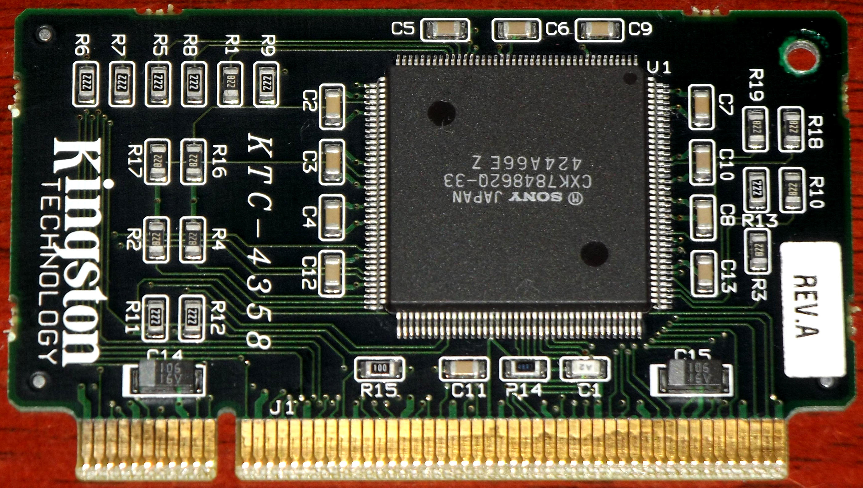
First post, by sander

User metadata
Rank Newbie
Rank
Newbie

I'm in the process of reverse-engineering the Compaq cache module for the Compaq Prolinea 4/xxx series, Presario 800 family and the ...(are there any other models?) This will definitely not work on the Deskpro 486 series as that needs the cache controller to be added to the module. I don't own a module myself, and the datasheet for the VL82C483 are nowhere to be found, but I believe the pinout of the VL82C483 is equal to the VL82C480 and VL82C481. This morning I mapped the 90 pin connector to the pins I found in the VL82C481 datasheet and everything seems to match. I only have three pins that I believe are unconnected and as there are no more cache pins left from the datasheet I think it's safe to say these remain unconnected (would be great though if someone could verify this on an existing module!). The VL82C48X memory controller logic is capable of accessing up to 64MB which would make a 256KB module sufficient and the VL82C48X seem to support this (afaik Compaq only had a 128KB module?).

All the effort that was put into the reverse-engineering of the FIC 486-GAC-2 proprietary cache module is of good use to me. So I made a head start by copying this project and using this as a starting point. The only big difference is my module uses 9 bits for the TAG cache although not stated in the datasheet the 9th bit is probably the DIRTY bit. This is something I need to change..

See the attached schematic for my progress, to be continued..

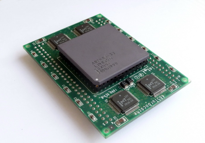
In my search for information on the VL82C483, I found a reference within a 1995 Cypress Data Book. Attached is a snippet from a Cypress cache module that's compatible with the VL82C483.

Reply 1 of 99, by pentiumspeed

User metadata
Rank l33t
Rank
l33t

Awesome!!

Compaq have buffers ICs on both Profinea MT motherboard is spares #: 197023-001 (VLSI 82C481)
This also have buffers on this Compaq Prosignia 4/33 (VLSI 82C483)

I plan to acquire the Compaq Prosignia 4/33 motherboard once money is available. The other board incoming is Profinea MT board from ebay a week or two ago.

Really like that fact is have dirty tag along with tag cache.

Cheers,

Great Northern aka Canada.

Reply 2 of 99, by rasz_pl

User metadata
Rank l33t
Rank
l33t
sander wrote on 2024-08-23, 11:01:

All the effort that was put into the reverse-engineering of the FIC 486-GAC-2 proprietary cache module is of good use to me. So I made a head start by copying this project and using this as a starting point.

Yay. This makes me very happy! Do you have github/gitlab/webpage I could link from my project page?

Compaq ProLinea 4/66 (164560-001) https://theretroweb.com/motherboards/s/compaq-prolinea-4-66
Compaq Presario 833CDS/850/850CDS/860CDS/866 (197023-001) https://theretroweb.com/motherboards/s/compaq-presario-800
Compaq Presario 700-900 series https://theretroweb.com/motherboards/s/compaq … -900-series-486

Updated my github with compaq examples 😀

https://theretroweb.com/motherboards/s/compaq … resario-cds-924 has same VLB cache slot (visible here https://wiki.preterhuman.net/Compaq_Presario_ … le:Cds924-3.jpg), but newer VLSI VL82C591/593 chipset

>definitely not work on the Deskpro 486 series as that needs the cache controller to be added to the module

do you mean 194380-001? this module posting.php?mode=quote&p=1286334
goes into ProSignia VS Server https://ardent-tool.com/media/PS2_MOST/ACRORE … PAQ/2005028.PDF https://www.digitaldungeon.be/digitaldungeon/ … gnia-vs_01.html
can see one installed in https://habr.com/ru/companies/selectel/articles/564668/

Alexandru Groza seems to be under impression his prolinea 4/66 requires some weird module, and not simple 197005-001 https://www.alexandrugroza.ro/microelectronic … -466/index.html You might want to mail him, he is down to F with some custom PCB design 😀

Researching about Compacs just now made me find need some help finding correct L2 cache RAM Good thread with some modules I didnt know about 😮

https://github.com/raszpl/FIC-486-GAC-2-Cache-Module for AT&T Globalyst
https://github.com/raszpl/386RC-16 memory board
https://github.com/raszpl/440BX Reference Design adapted to Kicad
https://github.com/raszpl/Zenith_ZBIOS MFM-300 Monitor

Reply 3 of 99, by pentiumspeed

User metadata
Rank l33t
Rank
l33t

The busy compaq chipsets using Ti and motorola chips boards of eariler 386 and 486 boards uses proprietary 64K cache module using also proprietary micron cache chips and intel 485 cache controller, around 1991-92 era. 64K Modules themselves are *Extreme Rare*, and as in to be speak, nearly extinct now. Parts especially cache chips for 485 are totally extinct especially, of those the non-standard cache SRAM chips made by micron to recreate 64K module with Intel 485 controller is now virtually impossible. Two types of modules using connectors that Compaq is using these 64K modules. One is daughter-board with two rows of connectors. And other one using slot connector.

The VLSI chipsets based compaq boards from 1994-1995 era are easier to do as long as can reproduce the PCB and does use easy to source chips and data sheet for VLSI chipset is there.
This would be a home run win if we can find VLSI 82C483 chipset datasheet. Good to have VLSI 82C481 chipset datasheet already.

If things go as planned and my budget comes in at end of month, buy the another compaq board with VLSI VL82C483 chipset and compare both boards using VL82C481 too.

I'd really wanted to find datasheet for the intel 485 cache controller and then understand what intel chose to use nonstandard cache chips for this.

Years ago in 93-94, one guy was looking for a 64K cache module as guy didn't know what to look for thus, I didn't know what he wanted. I had a similar cache module which is TTL buffers and standard cache chips. Sent it to guy and then returned to me, saying not compatible. Years later I understood why, he was looking for is called Intel TurboCache module which is 64K using 485 cache controller. I was sure that Intel was charging a leg and an arm for the 485 made demand for them so small, same issue with Compaq's as well. The difference is Intel's TurboCache module uses pair of dual row turned pin connectors.

Remember daughter-board means a module board is designed to be parallel with the main board (stack), thus, low profile. The module card and/or board is like a expansion card plugs into a slot, upright.

Cheers,

Great Northern aka Canada.

Reply 4 of 99, by pentiumspeed

User metadata
Rank l33t
Rank
l33t

The Compaq boards with VLSI chipset dates from 1994 or so and uses simpler cache module using TTL buffer and standard SRAM chips , *not* the intel TurboCache design. That is the context we are trying to recreate the cache module for VLSI chipsets: VL82C481 and VL82C483.

Another type that is not in context and only for purposes of difference information: VLSI chipset based compaq boards do not use these trubocache modules.
Intel TurboCache modules looks like this:
https://www.ardent-tool.com/misc/Turbocache_I … photo_angle.jpg

Cache controller:
https://www.ardent-tool.com/misc/Turbocache_I … photo_angle.jpg

Cache chips:
https://www.ardent-tool.com/datasheets/Micron_MT56C2818.pdf

Source: https://www.ardent-tool.com/misc/Turbocache.html

Also another word to show you what this extinct 64K cache module looks like; spare part: 141083-001.
Compaq also use this intel turbocache 485 as the card factor form with 64K size, as well for similar to 4/33i desktops (Deskpro/i and several models used in prosignia as well, with busy early boards.
https://www.amibay.com/threads/compaq-23052-a … o-4-66i.106879/

Two types of compaq very busy chipsets boards from 1991-1992 era that uses Intel 485 64K cache card using spares: 141083-001
https://theretroweb.com/motherboards/s/compaq … i-rev-1-p-n-002
https://theretroweb.com/motherboards/s/compaq … is-rev-3-p-n-00

Cheers,

Great Northern aka Canada.

Reply 5 of 99, by rasz_pl

User metadata
Rank l33t
Rank
l33t
pentiumspeed wrote on 2024-08-23, 18:08:
Intel TurboCache https://www.ardent-tool.com/misc/Turbocache_I … photo_angle.jpg Source: https://www.ardent-tool.com/misc/Turbo […]
Show full quote

Intel TurboCache
https://www.ardent-tool.com/misc/Turbocache_I … photo_angle.jpg
Source: https://www.ardent-tool.com/misc/Turbocache.html
spare part: 141083-001.
Compaq also use this intel turbocache 485 as the card factor form with 64K size, as well for similar to 4/33i desktops (Deskpro/i and several models used in prosignia as well, with busy early boards.
https://www.amibay.com/threads/compaq-23052-a … o-4-66i.106879/

Two types of compaq very busy chipsets boards from 1991-1992 era that uses Intel 485 64K cache card using spares: 141083-001
https://theretroweb.com/motherboards/s/compaq … i-rev-1-p-n-002
https://theretroweb.com/motherboards/s/compaq … is-rev-3-p-n-00

Nice, thank you. Adding to my list of proprietary cache modules reusing VL:B slot 😀 I think it was linked in need some help finding correct L2 cache RAM thread but picture link/upload is dead - google images was still showing ceramic package from cache when I found that thread.

https://github.com/raszpl/FIC-486-GAC-2-Cache-Module for AT&T Globalyst
https://github.com/raszpl/386RC-16 memory board
https://github.com/raszpl/440BX Reference Design adapted to Kicad
https://github.com/raszpl/Zenith_ZBIOS MFM-300 Monitor

Reply 6 of 99, by sander

User metadata
Rank Newbie
Rank
Newbie
rasz_pl wrote on 2024-08-23, 17:13:

Alexandru Groza seems to be under impression his prolinea 4/66 requires some weird module, and not simple 197005-001 https://www.alexandrugroza.ro/microelectronic … -466/index.html You might want to mail him, he is down to F with some custom PCB design 😀

And he is right 😉, he got himself a Deskpro motherboard (qvision vga) with a Prolinea enclosure, I know as I own both 😉

rasz_pl wrote on 2024-08-23, 17:13:

Updated my github with compaq examples 😀

That's a nice reference for 486 COAST modules!

rasz_pl wrote on 2024-08-23, 17:13:

do you mean 194380-001

That's the one!

rasz_pl wrote on 2024-08-23, 17:13:

Yay. This makes me very happy! Do you have github/gitlab/webpage I could link from my project page?

No project page yet, I will when I have something working.

pentiumspeed wrote on 2024-08-23, 17:34:

I'd really wanted to find datasheet for the intel 485 cache controller and then understand what intel chose to use nonstandard cache chips for this.

Cannot find it right now, but I believe there is a 485 design guide (as is for the pentium cache controller) on archive.org. While I was looking for the Sony cxk-78v4862 datasheet I came across that too.

pentiumspeed wrote on 2024-08-23, 17:34:

If things go as planned and my budget comes in at end of month, buy the another compaq board with VLSI VL82C483 chipset and compare both boards using VL82C481 too.

I'm almost certain they are pin compatible, would be good to get this verified.

Reply 7 of 99, by sander

User metadata
Rank Newbie
Rank
Newbie
rasz_pl wrote on 2024-08-23, 17:13:

Yay. This makes me very happy! Do you have github/gitlab/webpage I could link from my project page?

Awesome you are in this thread! As the form factor and pinout differs I believe I need to re-route everything?! In my search for a TAG replacement that's still in production (for now, I ended up with IS61C3216AL) I stumbled upon IS61C6416AL (1Mb, 64K x 16 SRAM). Do you think it's possible to replace the eight 32K x 8 SRAMs with two 64K x 16 SRAMs?

Something like this?

The attachment example.png is no longer available

Reply 8 of 99, by sander

User metadata
Rank Newbie
Rank
Newbie

After giving it a little more thought, would this work?:

The attachment new_design.png is no longer available

Reply 9 of 99, by sander

User metadata
Rank Newbie
Rank
Newbie

Never mind the 64k brain fart, VLSI designed it for x 8 chips.

Here is my 1.0 design, time to trace some tracks..

The attachment v1.0.jpg is no longer available

Reply 10 of 99, by rasz_pl

User metadata
Rank l33t
Rank
l33t
sander wrote on 2024-08-24, 08:19:
rasz_pl wrote on 2024-08-23, 17:13:

Alexandru Groza seems to be under impression his prolinea 4/66 requires some weird module, and not simple 197005-001 https://www.alexandrugroza.ro/microelectronic … -466/index.html You might want to mail him, he is down to F with some custom PCB design 😀

And he is right 😉, he got himself a Deskpro motherboard (qvision vga) with a Prolinea enclosure, I know as I own both 😉

the F?!?!
Alexandru Groza: "The internal mainboard documentation actually lists this machine as a Deskpro XE instead of a Prolinea. Furthermore, the Compaq Inspect program also reports the machine as a Deskpro XE. This leads me to think that these models were pretty similar and were produced in parallel."

indeed its 194362-001 on his pictures. What a mess 😮

Last picture on https://theretroweb.com/motherboards/s/compaq-deskpro-xe-486 shows it using Kingston KTC-4358 with same Sony chip as Prosignia VS 256KB Compaq 194380-001
On https://computer-retro.de/CPUs.html I found nice picture:
SONY-CXK784862Q-33-Kingston-Chip.jpg
Do you know/think if they are the same thing with Kingston just being second source? Glancing at power pins it seems to be the same thing.

sander wrote on 2024-08-24, 08:32:
pentiumspeed wrote on 2024-08-23, 17:34:

I'd really wanted to find datasheet for the intel 485 cache controller and then understand what intel chose to use nonstandard cache chips for this.

Cannot find it right now, but I believe there is a 485 design guide (as is for the pentium cache controller) on archive.org.

Intel A82485 datasheet https://www.datasheets360.com/pdf/4269492259628367834

sander wrote on 2024-08-24, 08:19:

While I was looking for the Sony cxk-78v4862 datasheet I came across that too.

Looks pretty cool, almost makes me think it could be easily adapted for 386 boards 😀 too bad the chip is unobtanium

sander wrote on 2024-08-24, 08:32:

As the form factor and pinout differs I believe I need to re-route everything?!

Yes, my PCB will be of little use to you other than getting an idea for spacing and capacitor placement. If you look in my module development thread I started by copying as much as possible from original module and then came the fun part of playing the puzzle solving for the unknown connections 😀 Last touch was modifying original by trying to move caps closer to Sram chips while staying close to original form factor.

sander wrote on 2024-08-24, 08:32:

In my search for a TAG replacement that's still in production (for now, I ended up with IS61C3216AL) I stumbled upon IS61C6416AL (1Mb, 64K x 16 SRAM). Do you think it's possible to replace the eight 32K x 8 SRAMs with two 64K x 16 SRAMs?

I also wanted to do this at first 😀 but separate /WE per 8bit chip means no

sander wrote on 2024-08-24, 11:30:

Never mind the 64k brain fart, VLSI designed it for x 8 chips.

afaik its more of a 386/486 CPU being designed this way, they needs to be able to write single separate bytes (BE0–BE3 signals) .

>v1.0.jpg
- I didnt even notice up to this point Compaq 197023-001 is shorter than FIC/AT&T/HP/Olivetti/full VLB slot. Bad move by Compaq, means they had to commission custom slots, suckers 😀
- and call side B what every other module and original VLB calls side A. This is most likely caused by shortening of the slot, thus they count pins from the other end.

1. Its standard practice to count even the missing/blanked pins, so your A12/B12 should be A14/B14.
2. You will have tons more space vertically than I did so you can fit all caps, one 1uF cap per chip as close to VCC pin as possible.
3. I would look inside the bios to make sure it does support dual bank 256KB cache configuration
4. IS61C3216 doesnt look to be readily available from reputable sources and might end up more trouble than two IS61C256
5. When routing PCB dont worry too much about keeping specific address/data order beyond A0 and keeping same 8 data pins per /WE line.

https://github.com/raszpl/FIC-486-GAC-2-Cache-Module for AT&T Globalyst
https://github.com/raszpl/386RC-16 memory board
https://github.com/raszpl/440BX Reference Design adapted to Kicad
https://github.com/raszpl/Zenith_ZBIOS MFM-300 Monitor

Reply 11 of 99, by sander

User metadata
Rank Newbie
Rank
Newbie
rasz_pl wrote on 2024-08-24, 14:24:

1. Its standard practice to count even the missing/blanked pins, so your A12/B12 should be A14/B14.

Good point, changed..

rasz_pl wrote on 2024-08-24, 14:24:

2. You will have tons more space vertically than I did so you can fit all caps, one 1uF cap per chip as close to VCC pin as possible.

True, although I'm trying to constrain myself to the original dimensions of the board, let's see where it get's me. Components will be on both sides. And after going through the FIC cache thread once again, I see I need to change the pads NOW 😉.

rasz_pl wrote on 2024-08-24, 14:24:

3. I would look inside the bios to make sure it does support dual bank 256KB cache configuration

Fair point. Although I have good hopes as this bios is shared with the older Deskpro which does support 256Kb. But then again the deskpro and prolinea don't share same chipset, this could very well be in a different section in the bios. From the VL82C481 datasheet it says there is ECh (Index Port) and EDh (Data Port), I should be able to easily find reference to these ports in assembly. Index register 19h (CACHECTL) has the following options:

The attachment cachectl.png is no longer available

heh, it even supports 1MB with a maximum of 64MB ram 😜. VLSI probably copied logic from the VL82C425 cache controller, which uses the same index register:

The attachment vl425.png is no longer available
rasz_pl wrote on 2024-08-24, 14:24:

4. IS61C3216 doesnt look to be readily available from reputable sources and might end up more trouble than two IS61C256

You're awesome, great point, I'll change it.

rasz_pl wrote on 2024-08-24, 14:24:

5. When routing PCB dont worry too much about keeping specific address/data order beyond A0 and keeping same 8 data pins per /WE line.

Although I should start with the longer traces. I'm such an amateur, my strategy always starts with slapping everything together and refactoring whatever comes along. Here is what I have so far:

The attachment progress.png is no longer available

Reply 12 of 99, by rasz_pl

User metadata
Rank l33t
Rank
l33t

I would probably start with original layout, or try to
- move buffers horizontally directly over the slot on A side
- move all SRAMS one over to the right so U1 ends up on right side of mounting hole, squeeze them closer
- put TAGs on the left
- leave /CE /OE /WE routing for last. You can swap banks and 8bit data groups around, it doesnt much matter which chips hold what as long as groups match.

Optimally for routing would be wiring TAG address lines together with Data chips. Caveat: I dont know if 244 buffers for Data but not Tag is only due to impedance (bus load limits) or also because TAG requires faster response (buffers introduce ~5ns delay), cant tell by looking at vl82c481 timing diagrams (pages 28/34).

https://github.com/raszpl/FIC-486-GAC-2-Cache-Module for AT&T Globalyst
https://github.com/raszpl/386RC-16 memory board
https://github.com/raszpl/440BX Reference Design adapted to Kicad
https://github.com/raszpl/Zenith_ZBIOS MFM-300 Monitor

Reply 13 of 99, by sander

User metadata
Rank Newbie
Rank
Newbie

You are right, although there are no DRC errors, I should probably redo it.. although I'm curious to test it.

The attachment no_drc.png is no longer available

Reply 14 of 99, by rasz_pl

User metadata
Rank l33t
Rank
l33t

Hey, if it fits, it sits!
Are you sure that vertical line of vias on all address lines going to buffers clears DRC?

https://github.com/raszpl/FIC-486-GAC-2-Cache-Module for AT&T Globalyst
https://github.com/raszpl/386RC-16 memory board
https://github.com/raszpl/440BX Reference Design adapted to Kicad
https://github.com/raszpl/Zenith_ZBIOS MFM-300 Monitor

Reply 15 of 99, by sander

User metadata
Rank Newbie
Rank
Newbie
rasz_pl wrote on 2024-08-26, 00:13:

Hey, if it fits, it sits!
Are you sure that vertical line of vias on all address lines going to buffers clears DRC?

Yes, DRC clears, based on your ruleset? I haven't looked at the rules yet, this is my first Kicad project and I'm too lazy to have a look at it, but I assume yours is JLCPCB compatible..

Would like to put some effort towards perfection. So I'm redoing it anyway. I believe the attached layout is with minimal vias. The SRAMs need more spacing though, so I'll move them a bit more to the right. But there are no vias in datalines, taglines and cpu lines to tag. The biggest amount of vias is from cpu (tag) lines to buffers, but I need vias for the buffers anyway..

The attachment new_layout.png is no longer available

.

Reply 16 of 99, by sander

User metadata
Rank Newbie
Rank
Newbie

It still needs a bit of a cleanup and four more capacitors, but after that I'll give this a first run.

The attachment first_run.png is no longer available

Reply 17 of 99, by rasz_pl

User metadata
Rank l33t
Rank
l33t

>Yes, DRC clears, based on your ruleset?

at a glance VIAs looked too close to each other. As a rule you should avoid rows of vias because clearance on inner layers cuts ground plane in two and messes impedance. I couldnt do much about it in the recreation as everything was too tight, but I tried moving vias/tracks as far apart where possible when data tracks ran under.

This layout works so much better!
Tons of space between buffers and sram to spread tracks as far apart as possible.
Whats happening with A15 under U11? if you swap if with A16 or A17 you can move U11 pin 17 via outside the pad.
I would play with data vias under SRAMs to pull them apart. For example I/O2 and I/O3 vias dont need to be under the chip at all, can all be moved below the chip routed over Ux chip designations - leaves more room for spacing out other I/O vias.
U9 pins 2-6 also try to spread those vias, for example pin 3 and 5 move vias over the chip and shift tracks so they dont go over clearance gaps.

https://github.com/raszpl/FIC-486-GAC-2-Cache-Module for AT&T Globalyst
https://github.com/raszpl/386RC-16 memory board
https://github.com/raszpl/440BX Reference Design adapted to Kicad
https://github.com/raszpl/Zenith_ZBIOS MFM-300 Monitor

Reply 18 of 99, by sander

User metadata
Rank Newbie
Rank
Newbie
rasz_pl wrote on 2024-08-27, 23:42:

Whats happening with A15 under U11? if you swap if with A16 or A17 you can move U11 pin 17 via outside the pad.
I would play with data vias under SRAMs to pull them apart. For example I/O2 and I/O3 vias dont need to be under the chip at all, can all be moved below the chip routed over Ux chip designations - leaves more room for spacing out other I/O vias.
U9 pins 2-6 also try to spread those vias, for example pin 3 and 5 move vias over the chip and shift tracks so they dont go over clearance gaps.

Thank you so much for your effort to review and to comment, greatly appreciated! I did the cleanup as promised and gave the overall design more 'air'. It now also clears DRC with teardrops and rounded tracks. I've tried (if understood correctly) to make the changes you proposed and did a first commit to github, would you be so kind and see if your comments still apply?

The attachment front_render.jpg is no longer available
The attachment back_render.jpg is no longer available

Reply 19 of 99, by rasz_pl

User metadata
Rank l33t
Rank
l33t

in "Draw Zone fills" mode you can see how every VIA carves out middle layers. The goal is to move vias apart so there are no big islands of no ground layer with fast signals going over/under them. This is the case currently on I/O signals.
Btw Im pretty sure you dont need to individually pull down unused sram data bits, you can gang them all to one pull down resistor.
Something like in attachement.

Edit: btw https://github.com/wichers/Compaq-Cache-Modul … 001_front_2.jpg hmm why did they put resistors after the buffers? and on 1OEs too, weird.

https://github.com/raszpl/FIC-486-GAC-2-Cache-Module for AT&T Globalyst
https://github.com/raszpl/386RC-16 memory board
https://github.com/raszpl/440BX Reference Design adapted to Kicad
https://github.com/raszpl/Zenith_ZBIOS MFM-300 Monitor