VOGONS


First post, by skafen

User metadata
Rank Newbie
Rank
Newbie

Hi All,

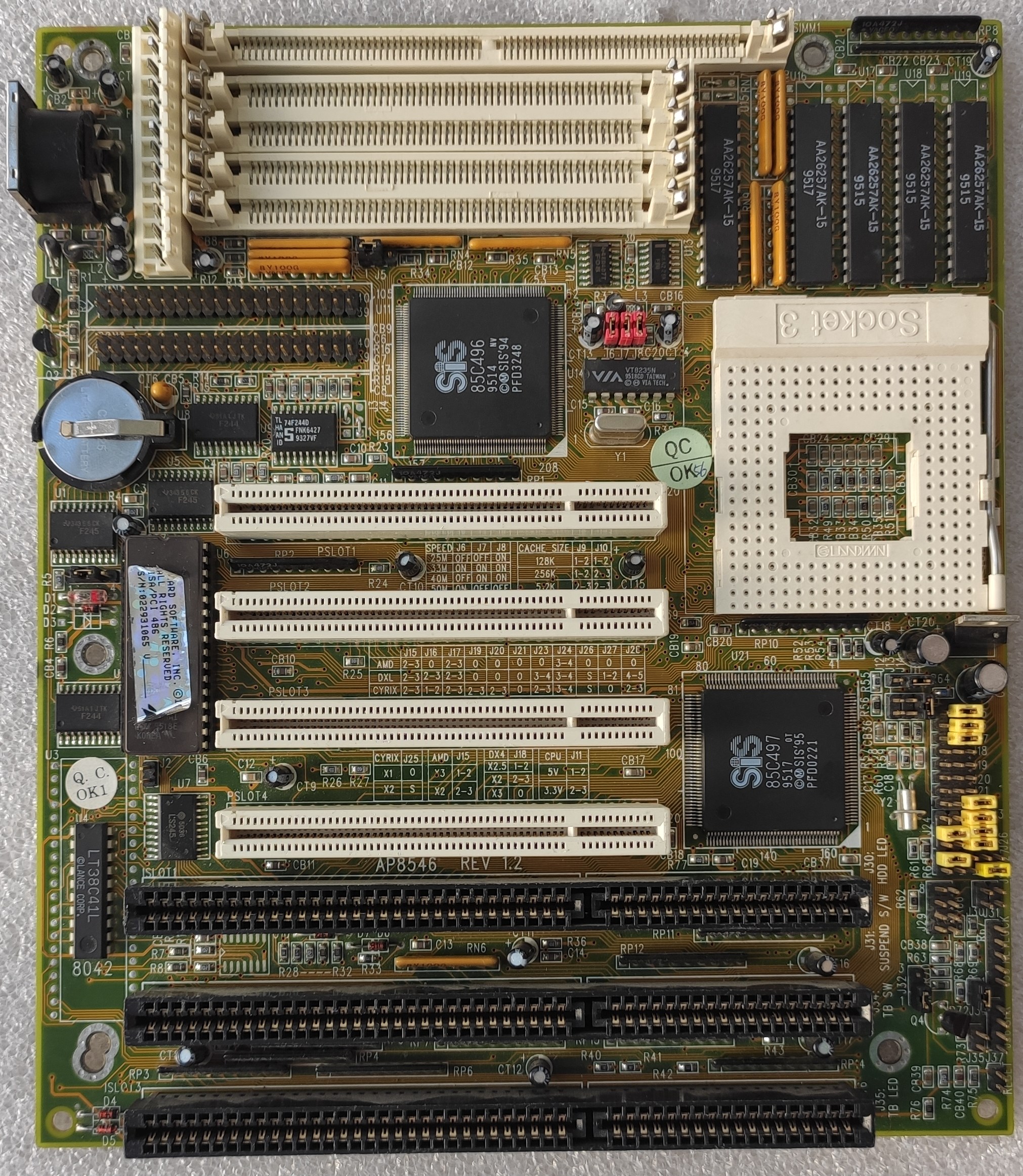
I have an Amaquest/Anson/Ansoon Technology Co. AP8548 Sis 496/7 PCI Socket 3 motherboard I acquired.

It works mostly (now) after fixing a few odd problems including dead RS232 line driver chips and ram sockets having gunk on them preventing simms from contacting correctly and at this moment is working quite well with an Intel P24C (writethough) Intel DX4 100 cpu... except for L2 Cache. It came with fake cache which I have removed and socketed but it does not work.

The board is listed on TRW https://theretroweb.com/motherboards/s/amaque … ology-co-ap8548 but seems to be an unknown with zero documentation on it.

I've figured out the CPU Voltage and FSB Speed jumpers and it came configured by the looks of it for an Intel 486DX. But the rest of the jumpers are a mystery including the L2 cache jumpers.

This is my third board of doing fake to real cache so am getting quite used to what to look for now but am a bit stumped on this one.

All cache sockets including the tag are getting normal looking signals on my oscilloscope compared to my last board I fixed which was a PCChips M912. It currently has a confirmed working 128K+Tag of 5 32kx8 15ns ISSI Chips and I cannot get it to recognise cache at all. The bios table says just WB under cache and speedsys/cache check etc all confirm no L2 cache.

Cache sizing appears to be done byJ14 and J15 which were pin-wired and I have replaced with headers and jumpers. Also it originally came with 4x passive resitor networks in U21/U22 which I have also now replaced with sockets and added 74F373N chips which also seem to have expected signals on them.

It's not the bios hobbled to disable cache as my M912 was. See PCChips M912 V1.7 Fake to Real Cache and new cache not recognised. I Suspect Bios version. for details on that as I've just tried the bios from a Jetway J446A on it which boots perfectly but says 256K no matter what.

I've got the Sis496/7 datasheet and am looking at that but it doesn't say how the L2 cache size detection actually works which would be useful to know at this point.

If anyone knows how this is done or has any info on this board at all I could really use the help with it.

Thanks

James

Reply 1 of 28, by skafen

User metadata
Rank Newbie
Rank
Newbie

Additional: I also added headers to JP10 and JP11 which are right behind the cache chips but trying diffrent configurations of jumpers there also either doesn't help or makes the board not post properly or at all.

Reply 2 of 28, by MikeSG

User metadata
Rank Oldbie
Rank
Oldbie

Assuming two TAGS, and one cache chip is right, there may be a third jumper in addition to J14, J15 to set.

Some of the other boards on retroweb with the same chipset have manuals, and have 3-4 jumper settings. The first two specify/multiplex 128, 256KB. The third specifies 512KB.

I would trace J32, to see if it is involved with the cache, and/or look for another solitary jumper.

Last edited by MikeSG on 2024-08-31, 12:14. Edited 1 time in total.

Reply 3 of 28, by skafen

User metadata
Rank Newbie
Rank
Newbie

MikeSG,

Thanks for responding. Why do you say two TAGS? The board definately only has the one 28-pin tag socket plus the 4 32-pin cache sockets.

I understand what you say about having more than the two jumpers though, but in looking through docs it seems to me that that most boards with 1 bank of cache like this one only have two jumpers and the third jumper is usually on dual-bank boards so you can select 256k as 4x 64kx8 or 8x 32kx8. Unless I'm wrong there.

Reply 4 of 28, by MikeSG

User metadata
Rank Oldbie
Rank
Oldbie

Sorry I got mixed up about the two TAGs.

This board has four jumpers to select one bank (4x 32x8kb). https://theretroweb.com/motherboards/s/a-tren … -atc-1425a#docs

But the other Amaquest board (with manual) only has the two jumpers. Written on the board between first & second PCI slots. https://theretroweb.com/motherboard/image/ap8 … 73403689772.jpg

So the two jumpers may be right.

Last edited by MikeSG on 2024-08-31, 12:16. Edited 1 time in total.

Reply 5 of 28, by skafen

User metadata
Rank Newbie
Rank
Newbie

J32 appears to also be a keyboard lock when shorted.

Reply 6 of 28, by skafen

User metadata
Rank Newbie
Rank
Newbie

Ah yes I see what you mean with the A-Trend board, I did think that the J10,J11 jumpers might serve that purpose but I've not been able to 'guess' any jumper config that works to get any cache at this point. I am looking at that other Amaquest board too, it looks like it could be an earlier predessor to this board, but the CPU slection jumpers are quite different sadly so not enough of a clue.

I've buzzed out the important pins on the cpu socket which vary between intel and cyrix and it looks like for intel writethrough none of them make any difference here. In fact the the board works including windows and PXE booting from a network card quite happily with only one single jumper present that is the voltdet pin. So I dont think the cpu selection jumpers here are what's upsetting the l2 cache here.

Reply 7 of 28, by MikeSG

User metadata
Rank Oldbie
Rank
Oldbie

You could try putting the resistor networks back (or jamming them in the sockets with the 74F373 chips to test). High speed signals often need pullups/downs.

Reply 8 of 28, by skafen

User metadata
Rank Newbie
Rank
Newbie

Already tried it. They fit find in the sockets on their own or as you say jamming in as well. Signals look okay. My scope isn't quick enough to show how clean the signals are at 33 or even 25mhz fsb but there's no obvious ringing or distortion of the waveforms.

Reply 9 of 28, by winnt5

User metadata
Rank Newbie
Rank
Newbie

I reverse engineered some of the circuitry related to the cache. As far as I know you must at least solder R103, R109, R102, R88, R86, R108 to make cache work. I don't know if there are more, so I am still reverse engineering it, and I don't know the exact resistance of these resistors, maybe you can just try 0 ohms since they are signal wires. R103 bridges OE# and KREX#, R108 bridges CE2 and KWEX#, the rest of them bridges each chip's CE1# and U15(74F08). They are for cache write byte mask logic.

Reply 10 of 28, by skafen

User metadata
Rank Newbie
Rank
Newbie

Oh hello thee winnt5! you got one too I'm guessing? Fingers crossed you figure it out. Mine is in storage right now so don't have it to hand to work on. But I'd love to get it going so will come back and try this.

Reply 11 of 28, by winnt5

User metadata
Rank Newbie
Rank
Newbie
skafen wrote on 2026-06-05, 11:16:

Oh hello thee winnt5! you got one too I'm guessing? Fingers crossed you figure it out. Mine is in storage right now so don't have it to hand to work on. But I'd love to get it going so will come back and try this.

Yes, I got one too. I almost gave up buying it since I have seen your post 🤣. I wish to know what you have learned about this board too! I think 74f373 is not needed because they are just used for buffering cache chip addresses. The original resistor will also let the signal go. I am ordering some 22 ohms resistors to have a try.

Reply 12 of 28, by skafen

User metadata
Rank Newbie
Rank
Newbie

Well I might be able to get my hands on mine next week, so if I do I'll try just solder blobbing those missing resistors to see if if makes a difference and I will let you know. In the mean time if you have any specific questions on this board please do ask away.

Reply 13 of 28, by skafen

User metadata
Rank Newbie
Rank
Newbie

Oh just worth mentioning as well that mine lost its original bios chip so I'm using a Jetway J446A bios in it currently which seems to work just fine.

Reply 14 of 28, by winnt5

User metadata
Rank Newbie
Rank
Newbie
skafen wrote on 2026-06-05, 16:20:

Oh just worth mentioning as well that mine lost its original bios chip so I'm using a Jetway J446A bios in it currently which seems to work just fine.

Is the ps/2 mouse working fine too? I'm using Lucky Star LS-486E Rev:D modified BIOS to avoid displaying fake cache. And ps/2 mouse works fine too.

Reply 15 of 28, by winnt5

User metadata
Rank Newbie
Rank
Newbie

Do you know the exact usage of jumper J8? It seems like a PCI clock frequency select jumper. But since I don't have an oscilloscope, I'm not sure which one is half frequency.

Reply 16 of 28, by winnt5

User metadata
Rank Newbie
Rank
Newbie

Oh I want to say that J10 and J11 seems not related to cache at all. They are weird and I think I should not touch them. Some of the pins are connected to the CPU and some of them even connects to specific CPU jumper. I cannot figure out any purpose on J10 and J11.

Reply 17 of 28, by skafen

User metadata
Rank Newbie
Rank
Newbie

The jetyway doesn't have a PS/2 mouse port so not tried it on the amaquest. I may try the Luckystar bios then.

I've not tried messing with PCI dividers etc as the board's permenant chip is an Intel DX4/100 writethrough which works fine with minimal jumpers e.g. for the writeback chips etc and just 33MHz clock so no need for any dividers. Mine is populated from memory without seeing it right now and I remember all the sysinfo numbers looked right for cpu/ram/cache speeds and also I test the video card speed with Dr Hardware 3.50 which is very good for showing if the video card speed is way off.

I didn't get much joy playing with J10/11 and I wonder if they only come in to play with odd CPUs like Cyrix which have different pins for their writeback caching etc. Or were never intended to be populated.

I can't tell you much more until I can get mine out at this point.

Reply 18 of 28, by winnt5

User metadata
Rank Newbie
Rank
Newbie

I have succeeded adding 512K cache. No other modifications are needed! Now even the 74f373.

Reply 19 of 28, by skafen

User metadata
Rank Newbie
Rank
Newbie

Congratulations that's great news. So all you had to do was bridge R103, R109, R102, R88, R86, R108 then? Did you use resistors?

What are your jumper positions for 512K on J14 and 15?

Thanks.