VOGONS


Gigabyte GA-486VF rev6 - issues with POD83

Topic actions

Reply 40 of 77, by rjbrown99

User metadata
Rank Newbie
Rank
Newbie

OK, so today my giant carton of every type of resistor showed up, so it was time for soldering.

To recap - the board uses an LT1085CT regulator near the CPU socket. I measured the original voltage at the LT1085 tab:

Original Vcore:
~3.437V idle
~3.438V under TESTCAB / SpeedSys load

So the regulator was stable and had essentially no droop, but it was only providing about 3.44V.

The LT1085CT pinout is:

Pin 1 = ADJ
Pin 2 = VOUT
Pin 3 = VIN
Tab = VOUT

I measured the existing feedback path:

Pin 1 / ADJ to Pin 2 / VOUT: ~0.618k ohms
Pin 1 / ADJ to ground: ~1.049k ohms

The lower feedback resistor is the blue SMD resistor marked 1051, which measured about 1.049k ohms and goes from ADJ to ground.

The mod was to add a resistor in parallel with the VOUT-to-ADJ resistor path, by soldering a through-hole resistor on the underside of the board between LT1085 pin 1 and pin 2:

Added resistor:
8.2k ohm, 1% metal film

Connection:
LT1085 pin 1 / ADJ <-> LT1085 pin 2 / VOUT

Do not connect to pin 3 / VIN.

Before soldering, the resistance between pin 1 and pin 2 was:

~0.618k ohms

The 8.2k resistor itself measured:

8.29k ohms

After soldering it across pin 1 and pin 2, the measured resistance between those pins dropped to:

~0.574k ohms

I started it up, and here's what the voltage regulator measured:

~3.599V

Which is just about perfect if I am to understand that this chip is rated for 3.6V maximum. I reassembled the board and confirmed the voltage was still around 3.59V after power-up.

Before changing jumpers back to 160MHz, I kept the system at the known-stable 3x40 / 120MHz setting and tested the mod:

40MHz bus
3x multiplier = 120MHz
Vcore ~3.59V
External cache enabled

That passed my TESTCAB copy-file test and SpeedSys normally, so the voltage mod itself did not appear to introduce instability.

I then changed only the multiplier jumper back from 3x to 4x:

JP24:
1-2 = 3x
3-4 = 4x

The system is now back at:

40MHz bus
4x multiplier
AMD-X5-133ADZ at ~160MHz
Vcore ~3.59V

Early testing looks promising so far. Both benchmarks have passed and there have been no crashes. I'm going to keep testing and we'll see where we wind up.

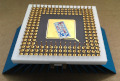
I had an Adrian Black style "IT FREAKING WORKED" moment already. Given that I have minimal electronics and soldering skills and had no confidence in what I was doing here, I'm surprised in a good way. This forum plus a bit of ChatGPT input might have unlocked the key to 160MHz for this board. A huge thanks to jakethompson1 and the other ideas on this thread so far. Woot!

Reply 41 of 77, by Chkcpu

User metadata
Rank Oldbie
Rank
Oldbie

Hi rjbrown99,

That is a nice mod you did, increasing the CPU voltage to 3.6V to get a stable 160MHz overclock on your Am5x86-133! I was less lucky with my Am5x86. Even at 4V I couldn’t get it to run stable 150 or 160MHz. 🙁
Anyway, I followed your endeavors with this GA-486VF board with interest. You already got great help from the community and i like to add some.

From your earlier Speedsys test pictures I noticed that you run the Am5x86 in L1 cache Write-Through mode. Note that the Internal Cache WB/WT option in the BIOS only works on Cyrix CPUs. Intel and AMD socket 3 parts don’t have software control for L1 Cache WB and need to have pin B13 pulled up to enable L1 Write-Back mode.
This is usually done by a jumper that connects this pin B13 to Vcc. Some additional CPU-chipset connections have to be made as well to get the WB mode work correctly.
In addition, the BIOS must program the chipset to enable the L1 Write-Back protocol signals.
Details about all this can be found in my old Am5x86 article:
http://www.steunebrink.info/amd5x86.htm

The 1994 Award BIOS doesn’t support the L1 WB logic for the DX4 and 5x86 CPUs, so you definitely need a BIOS update if you want the extra ~8% performance provided by L1 WB. But that’s the reason I’m writing. 😀

Did you see this thread from 4 years ago?
160mhz CPU on VLB Motherboard ?
I adapted an 11/28/95 SiS471 BIOS for the GA-486VS and you can download this GA-486VS Rev. J.1 BIOS from my second reply in this thread.
This BIOS supports all socket 3 CPUs, including the Cyrix 5x86 and Am5x86 in L1 cache WB and x4 multiplier mode. It’s also free of the year 2094 and 2GB HDD display limit bugs and supports IDE drives up to 8GiB.
Further down in this thread, TheMobRules uploaded a Rev. J.2 version of this BIOS with the Register 72h tweak that increases memory performance considerably.
I recommend this Rev. J.2 BIOS for a GA-486VF/VS upgrade.

Yes, the GA-486VF and GA-486VS are practically identical and use the same BIOS. The only difference between these boards is the type of RAM slots used (30-pin or 72-pin).

When running this 11/28/1995 BIOS, you still need the jumper settings for L1 Cache WB mode.
This is what @TheMobRules wrote in the above thread:

TheMobRules wrote on 2022-05-10, 08:24:
For future reference, here are the settings for both of these CPUs. Just follow the manual for an Intel DX4 and set these additi […]
Show full quote

For future reference, here are the settings for both of these CPUs. Just follow the manual for an Intel DX4 and set these additional jumpers:
• JP21: close 1-2 (this sets the hardware trap for WB L1 of the chipset)
• JP24: close 2-5 (to connect HITM# line from the CPU to the chipset) and 3-4 on the 5x86 only (it sets the DX4 multiplier to x2, which is x4 for the 5x86)
• JP30: closed (to pull the WB/WT# line high, enabling WB mode)
Note 1: there is no jumper for the INV pin, it seems to be permanently connected to Vcc, no jumper for CACHE# either
Note 2: if you set L1 to WB mode, DRAM Write Burst option in the BIOS needs to be disabled, otherwise it will hang when trying to boot MS-DOS

Hope this helps.
Cheers, Jan

CPU Identification utility
The Unofficial K6-2+ / K6-III+ page

Reply 42 of 77, by rjbrown99

User metadata
Rank Newbie
Rank
Newbie

Very interesting, thanks very much for that - I had not come across that limitation around the AMD CPU itself. Earlier in this thread it was suggested that the BIOS mod was needed and I have that done and the chip is just sitting to the side while I test and dial in each setting in the original BIOS. Didn't realize a pin change was also required. I'll read up on that in detail. And I didn't see your BIOS thread, but if it works for this board I'll pull that down and give it a try as well. That is super helpful and should improve my benchmarks.

Before I give it a try, my next step is to take this original bios and figure out the optimal settings with it - one at a time, with reboot and retry of my testing process and benchmarks. I want to land on a stable but performant baseline for 160 then graduate to the next round of changes. The BIOS you directed me to is 100% next on the list after the baseline.

I'm using an Adaptec AHA-2842A so the IDE bits aren't quite as relevant right now. I am planning to try the Adaptec BIOS mod for that as well to add large drive support.

I am also debating if I should buy 32MB of 50ns RAM from Atheatos and try it with 256KB of cache (assuming bank interleaving would be enabled). But that's for yet another day, I also have a fair amount of sanding and painting left to do for the case this is going into. Very hard to find cases in good shape so I'm doing a complete refurb of an intact but rusty purchase from eBay.

Oh, and I also have an IBM 5x86-100 on the way from Amibay - tested on a very similar Gigabyte board @ 120MHz. So I'll have two viable options to try for the CPU.

Reply 43 of 77, by rjbrown99

User metadata
Rank Newbie
Rank
Newbie

@chkcpu one clarification and follow-on question for you.

Intel and AMD socket 3 parts don’t have software control for L1 Cache WB and need to have pin B13 pulled up to enable L1 Write-Back mode.

Clarification: My motherboard has JP11: AMD CPU Selection Jumper. I have this open to indicate to the Board that it is an AMD CPU. As I understand your web page, this is the CPU/hardware side of enabling write-back. Nothing needs to happen to the actual physical pin B13 on the CPU itself.

Question: The above means that it's just the BIOS mod to enable write-back. And I did have that on a chip already, but I'm going to explore the one on your thread which fixes other issues. Any idea if you expect it will work on my board, as I have 30 pin SIMMS with 8 slots total whereas the GA-486-VS (which was the originating board of the BIOS on that thread) has 4 RAM slots? This was the issue I hit with the Mr Bios for this chipset, it was for a board with 4 RAM slots and wouldn't boot on mine.

I'll likely try it either way, but maybe another modbin change would be required on my board.

Reply 44 of 77, by jakethompson1

User metadata
Rank l33t
Rank
l33t

There is no broad reason to have a jumper for AMD CPU yes/no. What is probably happening is that AMD offered the DX4 in two pinouts. The original aka NV8T uses a custom pinout. The newer one aka SV8B aka Enhanced Am486 uses the P24D aka 486DX2-66WB pinout. The Am5x86 also uses the P24D pinout. It should be jumpered the same as an Intel 486DX2-66WB (except 3.6V instead of 5V) or the same as an Intel DX4WB (except 2x/4x instead of 3x).

Reply 45 of 77, by Chkcpu

User metadata
Rank Oldbie
Rank
Oldbie
rjbrown99 wrote on 2026-07-08, 00:18:

Very interesting, thanks very much for that - I had not come across that limitation around the AMD CPU itself. Earlier in this thread it was suggested that the BIOS mod was needed and I have that done and the chip is just sitting to the side while I test and dial in each setting in the original BIOS. Didn't realize a pin change was also required. I'll read up on that in detail.

Reading the above reply, I sense a confusion between L1 and L2 cache issues. Let me clarify.

The external L2 cache on the motherboard is fully controlled by the chipset. The L2 cache can operate in either WT or WB mode, as controlled by the External Cache WB/WT option in the BIOS Setup. The register 72h bit 2 tweak from earlier in this thread improves performance by enabling a dirty-bit in the Tag-RAM when the L2 cache operates in WB mode.

The internal L1 cache inside the CPU is controlled by the CPU itself and is completely independent of the L2 cache. So if the CPU supports it, the L1 cache can be operated in WT or WB mode, independent of the L2 cache WT/WB mode.
Most 486 CPUs only support the L1 cache WT mode but several Cyrix models, the Intel 486DX2WB (P24D), Intel DX4WB (has &EW markings), Intel POD83 (P24T), AMD Enhanced 486DX2, AMD Enhanced 486DX4, and the Am5x86-133 support both L1 cache WT and WB modes.
Except for the POD83, all above WB capable Intel and AMD models are switched from WT to WB via CPU pin-B13. This is where jumper JP30 on the GA-486VF/S is for. The motherboard manual indicates this jumper for the P24D only, but it functions the same on the other L1 WB capable CPU from both Intel and AMD.
(Note that the POD83 uses pin T1 for WT/WB selection.)

The only time when the chipset is involved in the L1 cache data handling, is when the L1 cache is in WB mode and the CPU has relinquished control to another busmaster controller like the DMA controller. A good example is the floppy disk controller that uses DMA to transfer its data to memory.
While during a DMA transfer the CPU is not active on the bus, it does “snoop” the bus. When the CPU senses that the DMA controller addresses a “stale” memory location for which it has updated data in its L1 cache which has not yet been written back to memory, it signals the chipset via its HITM pin (Hit Modified). This causes the chipset to force the DMA controller off the bus and grants the bus to the CPU to write the appropriate L1 cache line back to memory. After that, control is passed back to the DMA controller.
This CPU-DMA “dance” uses several signal lines between the CPU and the chipset, of which HITM is the most important, to ensure that cache coherency is always maintained. These signal lines are only used by L1 cache WB capable CPUs, and in addition the BIOS has to program the chipset to enable these WB protocol signals.

Both Intel and AMD WB capable CPUs use the same protocol and signals. So just as jakethompson1 indicated, don’t be fooled by an AMD CPU jumper and use the P24D jumper settings for the Am5x86, except of course for the CPU voltage and multiplier jumpers.

For the SiS471 chipset there are two additional chipset pin trappings that tell the chipset what kind of CPU it is dealing with.

The attachment SiS471 CPU Type Select trappings.png is no longer available

As shown in the above picture from the SiS471 datasheet, the CPU Type Select trappings use the DACK1# and DACK0# chipset pins. Although it is only indicated for the P24D and P24T, these pins must both be pulled high for any Intel and AMD L1 WB capable CPU, to enable the L1 WB protocol signals.
These trappings are usually controlled by 2 jumpers. On the GA-486VF/S I know one is JP21 that needs 1-2 closed. The other is probably JP11 that needs 1-2 closed as well.

I still believe that the 11/28/95 patch J.2 BIOS and the correct jumper settings will give you proper L1 cache WB support on your GA-486VF Rev 6.
I hope the above helps with that.

Cheers, Jan

CPU Identification utility
The Unofficial K6-2+ / K6-III+ page

Reply 46 of 77, by rjbrown99

User metadata
Rank Newbie
Rank
Newbie

Wow, thank you - that was quite a brain dump and I'm glad it will be on Vogons for others to find in the future.

My confusion was around write-through and write-back. I was initially viewing it as a single setting universally applied to the system, whereas you call out that write back is independently applied to L1 cache and L2 cache. I'm going to investigate jumpers and settings this week and report back. In the meantime my system is in pieces as I am in process of painting the case and power supply.

Let me ask a follow-on question! My Adaptec AHA-2842A card has a jumperfor write-back as well. How does that relate (or not) to the write-through and write-back jumpers for the L1 and L2 cache? I am assuming it is yet another independent application of the concept but specific to the storage controller itself.

Thanks again, super helpful.

Reply 47 of 77, by jakethompson1

User metadata
Rank l33t
Rank
l33t

Because your AHA-2842 bus masters--reads or writes directly to memory without going through the CPU--when using a write-back internal cache, the CPU needs the ability to hijack the AHA-2842 from reading stale information in memory if there is more up-to-date (dirty) data in L1 cache.

Because internal write-back cache was retrofit to later 486 systems, the jumper is probably there in case the VLB pins involving write-back internal cache are wired incorrectly (e.g., grounded or pulled-up) on the motherboard, if they didn't exist yet when the motherboard was manufactured.

Reply 48 of 77, by rjbrown99

User metadata
Rank Newbie
Rank
Newbie

Ha, so I finally got my case and everything else painted so back to the config. The J.2 bios seems to work, at least with 64mb of ram in 4 of the 30 pin sockets. I haven't tried with the full 128mb yet but so far it booted and seemed OK. It was the only BIOS I tried to properly identify the AMD CPU and its configured speed (at the boot screen).

I read the above thread, went back around to map out the jumpers, and finally was going to test with L1 writeback. One of those changes is to jumper JP30 for P24D writeback. And then I looked at JP30 and its empty pads staring up at me. FFS.

I had previously ordered a proper soldering station and tips so once they come in within the next week or two I'll remove the existing paste and solder down some pins so this can become a real jumper. Later revisions of this board seem to have the jumper in place - I found a picture of Rev 8.B online and it had the jumper pins.

All I can keep thinking to myself is how did anyone even remotely try to do this in the 1990s without forums like Vogons and YouTube videos to learn from. Thanks for listening folks, the journey continues.

Reply 49 of 77, by rjbrown99

User metadata
Rank Newbie
Rank
Newbie

Update on my journey as of late.

So I came across one of these boards for sale - revision 8B! This has the built-in JP30 and the manual states that "This option is valued from P.C.B. REV.8A & BIOS July, 12 1994 or later." So I thought that perhaps the 8B board would have better luck with the POD and/or cache.

I received the board and had to replace the broken keyboard adapter with a new one and also remove the leaky battery and replace it with a Not-A-Varta. The battery had leaked a small amount around one of the mounting holes so I gave it a liberal treatment with white vinegar (top and bottom) and then washed it off. None of the traces look to be visually damaged, it was localized to just the one hole.

Then I dropped in a post card, verified jumper settings for the Am486 DX4-100 that the board came with, and powered it on. The post card just shows the code "CF4F" OR "4FCF" - no beeps, and does not cycle through any part of the early stage boot. I powered off and tried a few more things. Tried known-good memory, same result. Booted with CPU but without memory, same result. Swapped CPUs to a DX4ODPR100 and set the board back to 5V (to eliminate the voltage regulator as an issue), no change. I pulled the BIOS and dumped it, and it was a clean read and the chip is fine. I then pulled all of the cache chips and TAG SRAM, same result - CF4F or 4FCF. And when I use the word "or" there - on one boot it might show CF4F, on another it might show 4FCF. One of those two values appears on each successive poweron but they don't change at all, it's a static reading once power is applied.

That's where I stopped for the weekend. I'm going to pull out the multimeter and do some voltage tests to see what I can find. If they test out OK I'll break out the microscope and start following traces around. I'd prefer not to revert to the fiberglass pen / removing solder mask / testing traces / re-masking. But I'll go there if needed.

I just thought I'd recap in case someone here says "ah hah - I have an idea what CF4F/4FCF might mean and help narrow the field of potential problems!

Edit: the "reset" LED on the post card is also lit, so I'm looking to see if there is an issue with either that run or with the tantalum cap that is on the path. No caps are visibly blown on the board.

Post codes are here on page 56: https://theretroweb.com/motherboard/manual/48 … d0110265622.pdf

Reply 50 of 77, by jakethompson1

User metadata
Rank l33t
Rank
l33t

If you can post high-resolution images of the front and back, there could be a trace scratched through. I had a trace in back of the the SIMM area scratched through once, and it took me quite a while to narrow it down.

Reply 51 of 77, by rjbrown99

User metadata
Rank Newbie
Rank
Newbie
jakethompson1 wrote on 2026-08-10, 05:43:

If you can post high-resolution images of the front and back, there could be a trace scratched through. I had a trace in back of the the SIMM area scratched through once, and it took me quite a while to narrow it down.

My friendly AI model is suggesting we test whether the CPU is being held in RESET by probing the reset pin from the under side of the board. That would narrow it down to focusing on why reset isn't being released. Sounds plausible.

I have a microscope and I'll start looking at traces after a bit more work with the meter. I also ordered some capacitors so I can replace the one that I know is on the reset path. I don't have a high resolution enough camera to post something here that would be useful.

Reply 52 of 77, by MikeSG

User metadata
Rank Oldbie
Rank
Oldbie

Code CF is keyboard controller related. Maybe there is a broken trace nearby, or needs to be reinserted in the socket.

Reply 53 of 77, by rasz_pl

User metadata
Rank l33t
Rank
l33t
rjbrown99 wrote on 2026-08-10, 06:16:

My friendly AI model is suggesting we test whether the CPU is being held in RESET by probing the reset pin from the under side of the board. That would narrow it down to focusing on why reset isn't being released. Sounds plausible.

On one hand CPU should be running if you are getting POST codes.
On the other "CF4F" OR "4FCF" are not valid POST code sequences for this Award bios. To be more precise '4F' is (POST_4F_Password), but it can only happen somewhere in the middle of hardware initialization after at lest 30 other post codes, long after VGA output got enabled.

>replace the broken keyboard adapter with a new one

Same model? KBCs do control reset, either directly or going thru chipset. measure Pin 21 of KBC.

On the third hand ;P no ISA transactions should ever take place with active RESET signal. Either POST card is defective or something very wrong with the chipset - best case scenario lifted pins or maybe somehow (tho I dont know how in a reset) bad connections on ISA slot.

MikeSG wrote on 2026-08-10, 11:08:

Code CF is keyboard controller related. Maybe there is a broken trace nearby, or needs to be reinserted in the socket.

I disassembled the BIOS https://github.com/raszpl/Award_4.50G_BIOS, cant find a place where it would ever send CFh.

https://github.com/raszpl/sigrok-disk FM/MFM/RLL decoder
https://github.com/raszpl/FIC-486-GAC-2-Cache-Module (AT&T Globalyst)
https://github.com/raszpl/386RC-16 ram board
https://github.com/raszpl/Zenith_ZBIOS Zenith Z-386 MFM-300 ZBIOS disassembly

Reply 54 of 77, by TheMobRules

User metadata
Rank Oldbie
Rank
Oldbie
rjbrown99 wrote on 2026-08-10, 02:36:

I received the board and had to replace the broken keyboard adapter with a new one

By "keyboard adapter" you mean the KB controller chip or the DIN connector? If it's the chip, keep in mind that there are different variants that are not 100% compatible with one another. For this board in particular, there are some jumpers that allow you to set the type of KBC chip being used. There is a video from Necroware where he had to replace the chip on this Gigabyte board and he explains the issue in great detail:

https://www.youtube.com/watch?v=IexvdgG_Zi0

Reply 55 of 77, by rjbrown99

User metadata
Rank Newbie
Rank
Newbie

Thanks for the input everyone, very helpful in my next set of tests. I'll focus on the keyboard area and report back.

When I say replaced the keyboard adapter I mean the image below. I soldered a new one into place as the old one had pins that were broken off. I performed the same fix to the original board for the same reason.

I did not touch any chips on the board at this point, just soldered the new DIN and hit it with white vinegar to get rid of the corrosion.

The link to the video was a big help, but not for the reason you might expect. I had the post card in backwards, so yeah that's not great. After swapping it to the correct orientation it no longer displays those codes, and instead just 4 dashes.

The lights on the post card are:
-12V on
+12V on
+5V on
+3.3V on

CLK on
IRDY off
FRAME on
RESET off

Seems like a logic probe would be helpful at this point and it's the one tool I don't have. It's now on order, will be here next week. In the meantime if anyone has ideas I'm all ears, thanks!

Reply 56 of 77, by rasz_pl

User metadata
Rank l33t
Rank
l33t
rjbrown99 wrote on 2026-08-11, 03:21:

When I say replaced the keyboard adapter

so connector 😀
look at this cure lil 20-pin LANCE LT38C41L keyboard controller!

rjbrown99 wrote on 2026-08-11, 03:21:

I had the post card in backwards, so yeah that's not great.

fascinating that it did anything at all when inserted backwards 😮

test it in another mobo, might be fried now, might never worked to begin with
since ISA slot address lines are wired directly to bios chip it might have fried BIOS, or even chipset
do you have mans of reading back bios chip to validate if its still ok?

rjbrown99 wrote on 2026-08-11, 03:21:

Seems like a logic probe would be helpful at this point and it's the one tool I don't have. It's now on order, will be here next week.

what do you mean by logic probe? those pens with lo hi leds? imo its junk, multimeter shows more data (actual level) in voltage mode
a scope or even a $5 logic analyzer on the other hand would be huge

good scope diagnostic steps listed: https://forum.vcfed.org/index.php?threads/gig … iagnosis.60265/

https://github.com/raszpl/sigrok-disk FM/MFM/RLL decoder
https://github.com/raszpl/FIC-486-GAC-2-Cache-Module (AT&T Globalyst)
https://github.com/raszpl/386RC-16 ram board
https://github.com/raszpl/Zenith_ZBIOS Zenith Z-386 MFM-300 ZBIOS disassembly

Reply 57 of 77, by rjbrown99

User metadata
Rank Newbie
Rank
Newbie

When I say logic probe - yes I mean a simple probe that reads high/low. I don't have an oscilloscope yet but I have one on the way from China. I do have a multimeter.

I tested the POST card in the working board and it came up and read the values as expected, no issues. I also dumped the BIOS again and verified the chip, both were successful. So I don't think the card or BIOS are issues, but certainly not ideal that it just shows ---- when powered on.

Reply 58 of 77, by rasz_pl

User metadata
Rank l33t
Rank
l33t

good news about the post card. Does reset led react to pressing mobo Reset button?

stick a needle in cpu socket pin C16 hole responsible for reset, put multimeter in voltage move, stick black probe into molex ground black wire, red probe to needle, press/short Reset pins on mobo, see if anything changes

https://github.com/raszpl/sigrok-disk FM/MFM/RLL decoder
https://github.com/raszpl/FIC-486-GAC-2-Cache-Module (AT&T Globalyst)
https://github.com/raszpl/386RC-16 ram board
https://github.com/raszpl/Zenith_ZBIOS Zenith Z-386 MFM-300 ZBIOS disassembly

Reply 59 of 77, by rjbrown99

User metadata
Rank Newbie
Rank
Newbie

Update on the GA-486VF Rev. 8B troubleshooting.

I went through the board pretty thoroughly tonight. Current configuration is an Intel DX4ODPR100 at 33 MHz bus, and I did a full jumper audit against the manual. All documented jumpers appear correct, including JP5/6/7 ON, JP8 1-2, JP11 closed, JP18 closed, JP20 2-3, JP21 2-3, JP24 open, JP29 open, JP36/37 closed, and the VLB delay jumpers at 1-2. Cache is currently removed; its normal setting was JP1 ON / JP2 ON / JP3 OFF / JP4 2-3.

The POST card is now definitely installed in the correct orientation. The earlier CF/4F codes were bogus because I originally had the card backwards, so those can be disregarded. With it installed correctly I consistently get ----. LEDs show -12V, +12V, +5V and +3.3V present; CLK on; RESET off.

Reset circuitry seems to be working. I connected the case reset switch to J6: the POST-card RESET LED turns on immediately while the button is held and goes off immediately upon release.

The BIOS EPROM is a TMS27C512. I dumped it successfully with MiniPro. The image is 64 KB, has the expected Award 4.50G/Gigabyte GA-486VF Rev. 8B identification and a valid-looking reset vector. The BIOS chip also measures 5 V between VCC and ground while installed.

I also investigated the area affected by the old Varta battery leakage. The corrosion had previously been cleaned with vinegar/IPA. I traced quite a few relevant traces and vias with the multimeter and haven't found an open in the corrosion-affected area so far.

The replacement 5-pin DIN keyboard connector got quite a bit of attention. Pinout is standard DIN:

1 = KBDCLK
2 = KBDAT
3 = KBRST/reserved
4 = GND
5 = +5 V

With the connector removed I traced KBDCLK from DIN pin 1 through L2, vias, the unused large keyboard-controller footprint and farther into the keyboard-controller circuitry. R7 measured 4.70 kΩ and R8 4.72 kΩ. KBDAT through L3 also had continuity through the portions checked.

Powered the board again afterward: still ---- on the POST card.

I also tried a MiGron ISA/AT clock measuring card. It reports 7.16 MHz consistently at power-on. So there is a measurable ISA bus clock even though the POST card remains at ----.

At this point the basic power, jumper configuration, reset operation, BIOS ROM contents/power, DIN connector, and a reasonable portion of the corrosion-area continuity have been checked.

Next step is probably dynamic signal testing. The Elenco LP-560 logic probe shows up Monday. My plan is to start at the 27C512 BIOS and check /CE and /OE after releasing RESET, then address/data activity. That might tell us whether the CPU/chipset is actually fetching the BIOS at all.

I also have an oscilloscope on order from AliExpress, so might take another 1-2 weeks to arrive. Not sure there is much else I can do without the probe and/or scope, but I'm open to ideas. After tonight I'm more confident that the keyboard adapter and lines are OK.