Several pages ago (around the beginning of this year) i went through bunch of dual Slot1/2 (Pentium III) motherboards in attempt to identify the best ones and build a badass graphics / software_development workstation.
This initiative is reflected in the next posts:
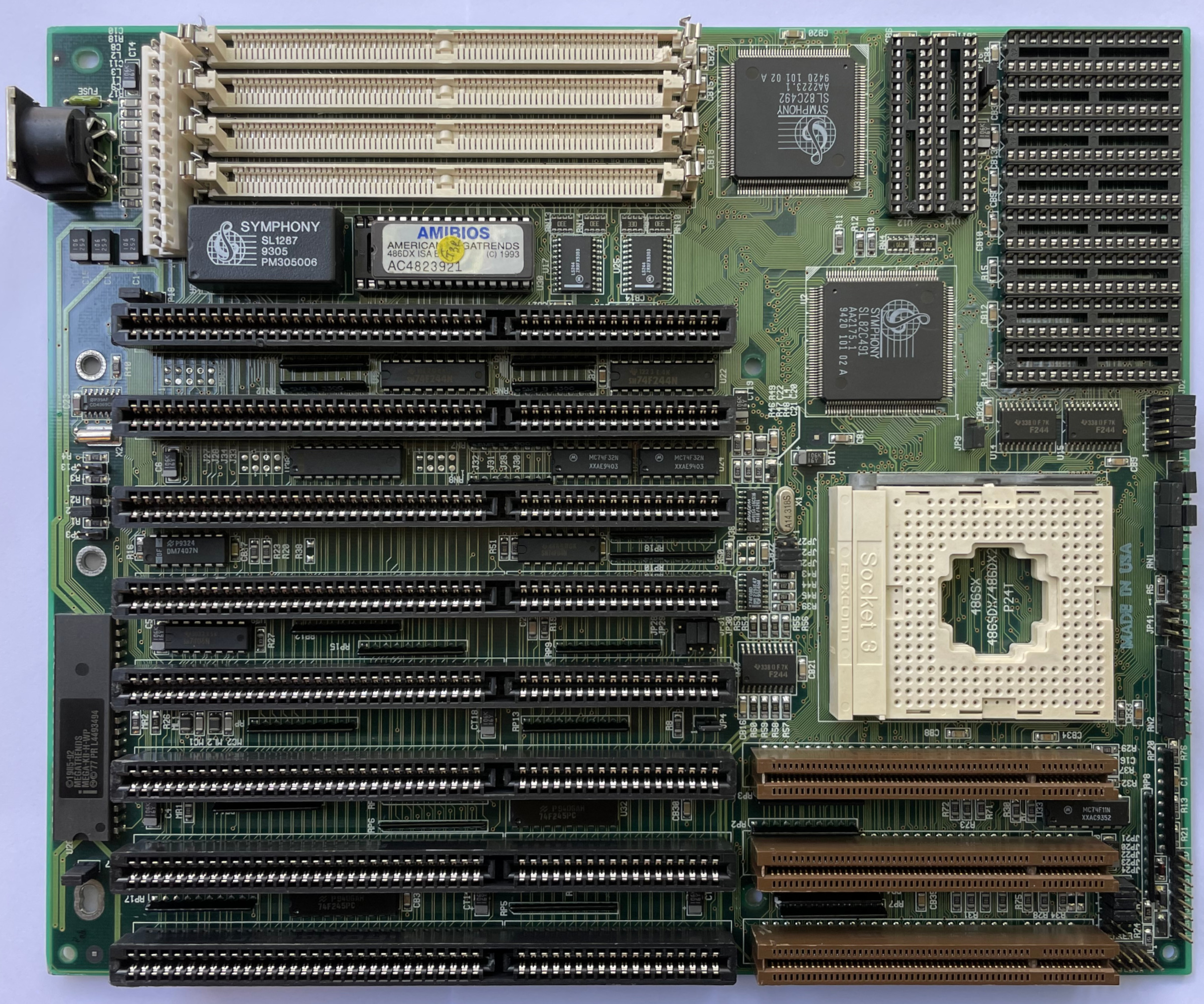
Supermicro S2DGE, Tyan Tiger-133, Asus P2B-D
OR840 (IBM Intellistation M Pro, Type 6868)
OR820 (Dell Optiplex G300)
(there were 2 more BX440 boards from Gigabyte and Soyo that were discarded early on)
The last one from the OR800 series was an interesting case and took longer, because i put quite a bit of effort to work around some issues with it.
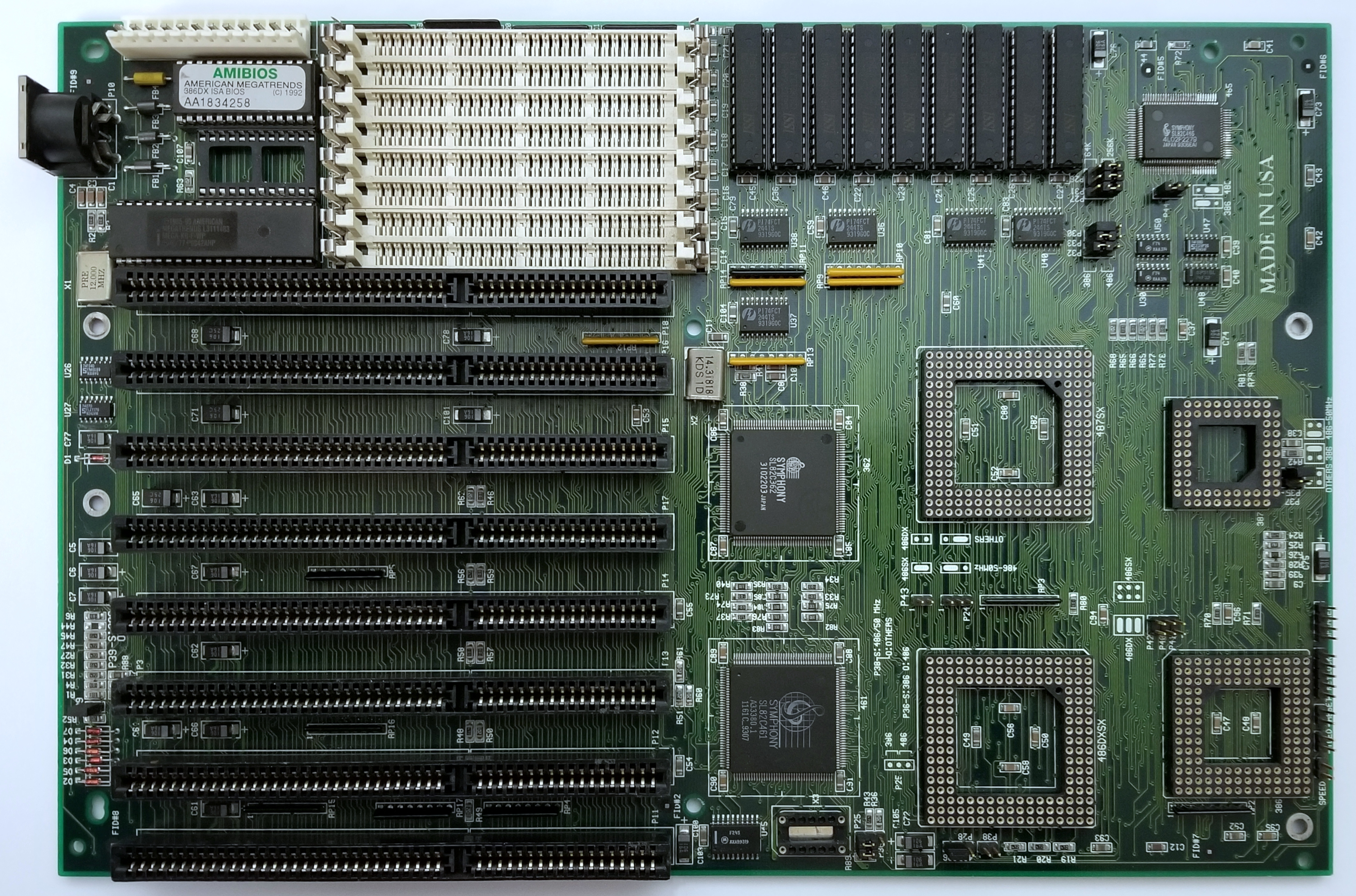
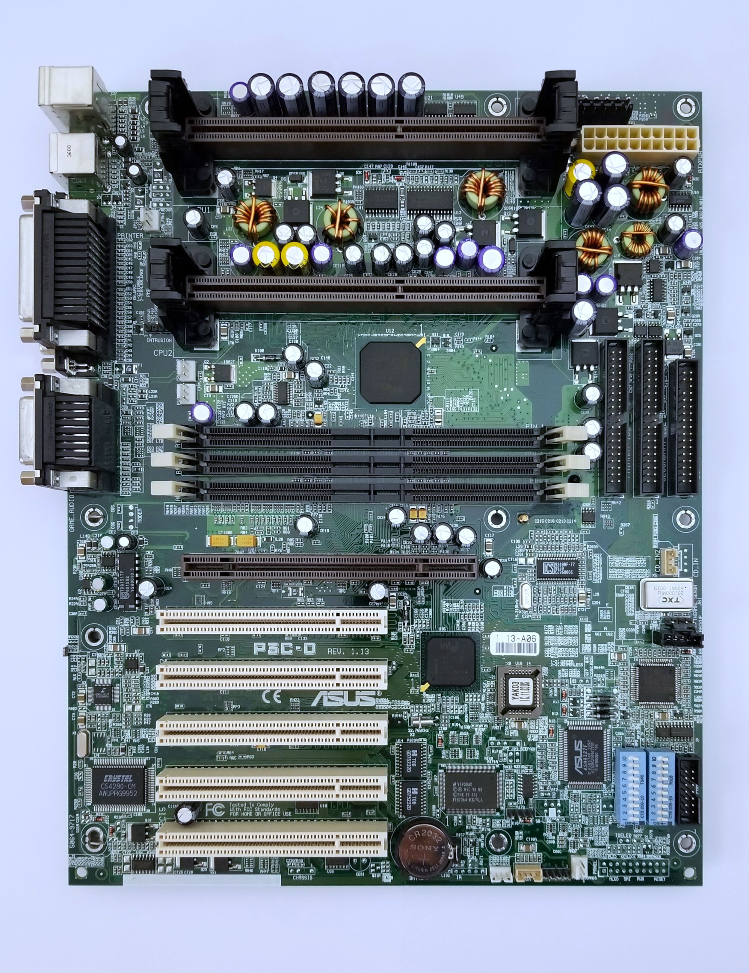
Asus P3C-D (rev. 1.13-A06) / HP Kayak XM600 - a bitter-sweet experience.
Where to start really ?
Assembly is of very high quality.
Standard ATX layout, components and connectors - something that is worth mentioning, as most dual CPU OR8## implementations out there are weird - unusual formats, custom connectors, require specific PSUs, etc.
On-board UltraDMA/66 controller, Crystal CS4280 PCI audio, IR.
AGP Pro slot.
Clock generator that supports up to 180MHz.
That clock gen suggests that the system is meant for overclocking, something that is common for many Asus products and something that i badly wanted to try, but ...
... the HP engineers who built it into the Kayak XM600 were on very different opinion.
All OC-related settings are omitted from HP's customized BIOS.
DIP switches cannot go past 133MHz FSB, regardless of what ASUS's manual says.
Custom HP POST process forces memory check that takes very long time with 1Gb of RAM installed. It really tests your patience.
And so on.
So i spent time trying to circumvent the imposed limitations.
Unsoldered some the custom HP chips and tried to rewire the circuits. That never worked. It was a shot in the dark to start with.
Installed a second DIP switch package, where the default one (from Asus) would have been. That didn't change the resultant behavior of the switches.
Socketed the EEPROM, burned the original ASUS bios on another chip, but board didn't light up with it.
Tried to force higher FSB by hard-wiring the clock-gen. That didn't go well too.
Basically, i was beaten back at every step and 2 weeks ago officially surrendered.
Disappointing.
So, going with the base package that HP thinks is what i deserve:
2 x Tualatin-S 1400/133/512
Quadro FX4000 (NT4) and Quadro2 Pro (DOS)
2x512Gb 40ns RIMMs + terminator, at base 100MHz speed.
3COM LAN card.
In this configuration - no complains - everything works as advertised.
HP's control panel.
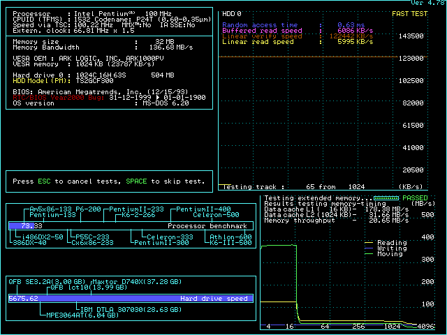
Here is what speedsys says:
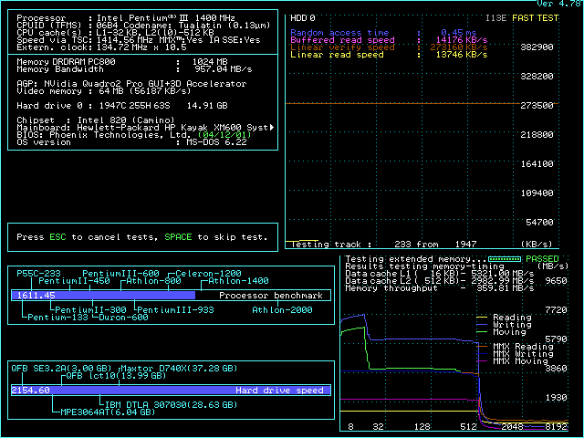
Looks good overall. Disk i/o is not that great.
The standard set of benchmarks.
Compared to Asus P2B-D at the same CPU/FSB/AGP frequencies and video cards.
Gray bars represent peak perf with P2B-D at 1575/150/48.
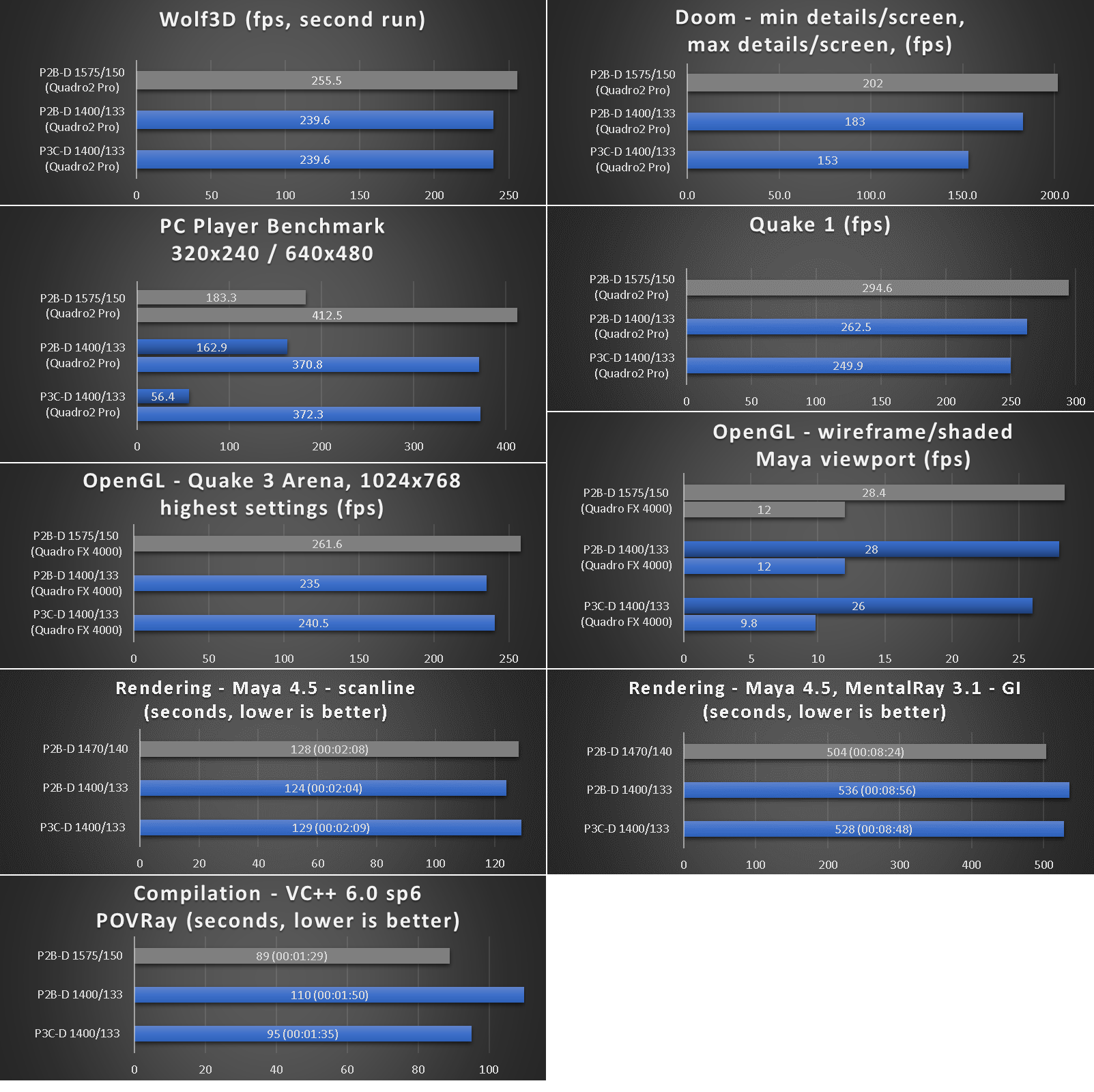
Couple of things to notice:
- Global Illumination rendering test, C++ compilation test - P3C-D is clock-to-clock faster than P2B-D.
- OpenGL Quake3 test, scanline rendering test - clock-to-clock things are on par. Keep in mind that the scanline rendering test is heavily influenced by disk i/o (large shadow maps). I used the built-in UltraDMA/66 controller for the tests instead of Promise ATA/100. I am pretty sure that the 5 seconds difference would be erased by ATA/100 in the loop.
The first link in this post touches on turning P2B-D/BX440 into something that is unmatched by any other P3 system.
It takes next-next gen P4 hardware to outdo it.
If HP didn't butcher the P3C-D board - it could tell a story with potentially unexpected end for BX440.
Too bad.
---
OR800 hardware had limited market window back in the day, so Vanilla Asus P3C-D motherboards are rare today. Never saw one for sell really.
Online searches don't reveal anything conclusive about their qualities.
Curious how well they overclock.
Any hints ?