Reply 1800 of 2513, by WJG6260
- Rank
- Member
@pshipkov
Excellent work on the 386 hardware. Your results are invaluable and your time is much appreciated! Thank you for this Herculean effort-it has been quite exciting, to say the least, and I am very interested in seeing where your next stop is hardware-wise!
Thank you for doing this indeed! 😁
----
Before sharing my saga with the ALD PCI5433 below, I just want to briefly mention something interesting. The other day, I was working on my Soyo 4SA2. It had a mangled 72-pin SIMM socket, which I promptly replaced. It's been fine since, and I could not help but notice something fascinating, regarding the reason-perhaps-for its average performance: the Dirty TAG is not enabled! CTCM 1.5b clearly shows this, regardless of the L2 size and BIOS settings for WB. As long as WB L2 is enabled on this board, it is in always dirty mode! In other words, it suffers from the same problem as the ASUS VLI, pre-modded BIOS by Feipoa.
Using MCSIS496.COM, a tool written by a member here that can modify chipset registers of the SiS496 BIOS, I set out to remedy this. I haven't gone so far as to mod the BIOS (yet), but for now, this suffices. I wrote a small script in batch that calls MCSIS496, enables the 7+1 TAG configuration by modifying Register 42h, BIT 2. Setting that to 1 enables such a configuration. The dirty TAG cannot immediately be enabled, otherwise the system will hard-lock. I presume that the cache has to be flushed first, so, in an attempt to do such and verify the results at the same time, my script calls CTCM 1.5b (which I keep in the MARKS folder of DOSBENCH, but this can be changed). It then runs CTCM to demonstrate that the TAG is off and cycle the cache, and then calls MCSIS496.COM to set BIT 3 of Register 42h to 0, which enables the dirty TAG operation. CTCM 1.5b is called once again, to demonstrate higher speeds, and then the script quits. It works well enough. I've attached the files here, if anyone wants to give it a go. Just be sure to either edit the batch script to call CTCM 1.5b at the location where you keep it, and the same goes for MCSIS496.COM.
The script I wrote auto-sets CTCM 1.5b for your L2 cache amount based on a selection menu. Do note that CTCM 1.5b requires the /l2 flag to properly detect 1024k L2 (and sometimes even 512k).
----
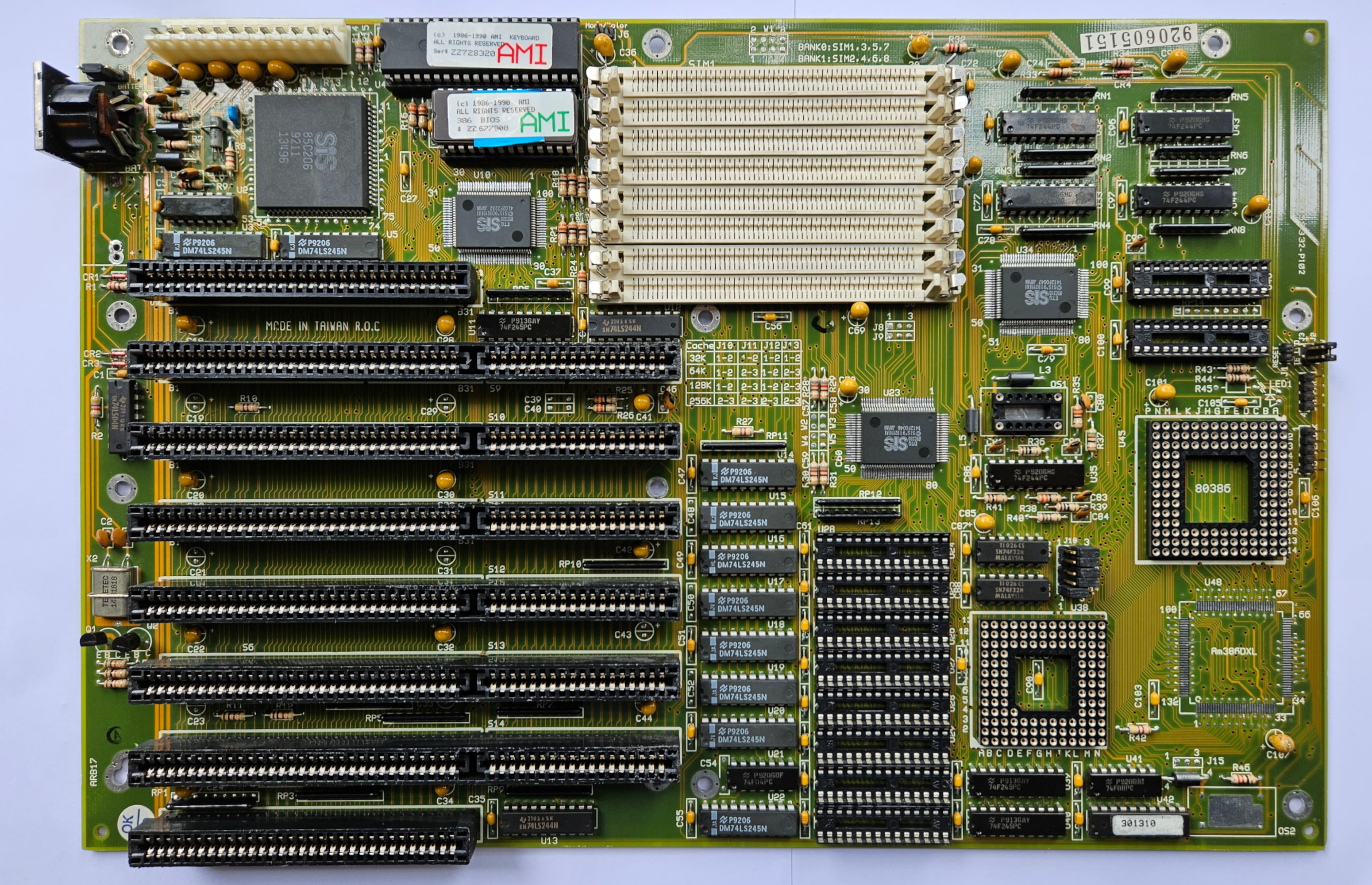
A while ago, I happened upon perhaps one of the oddest 486 boards to date.

This story starts with ALD-the manufacturer of this board. ALD's designs are perhaps some of the strangest out there, notably defined by cheap, highly-integrated assemblies. One rather infamous ALD board is the VL4200, a single-chip VLB board based on the 93C413 chipset. It supposedly can support cache, but comes laden with fake cache ICs and does not seem to support real cache, even when modified.
I realized this thing needed a manual, so I emailed ALD. Their website still exists, and it looks to be straight out of 1997. Their support actually had the manual, and it has since been uploaded on TRW as a PDF. Talk about a good (and quite weird) start to an otherwise fascinatingly strange saga.
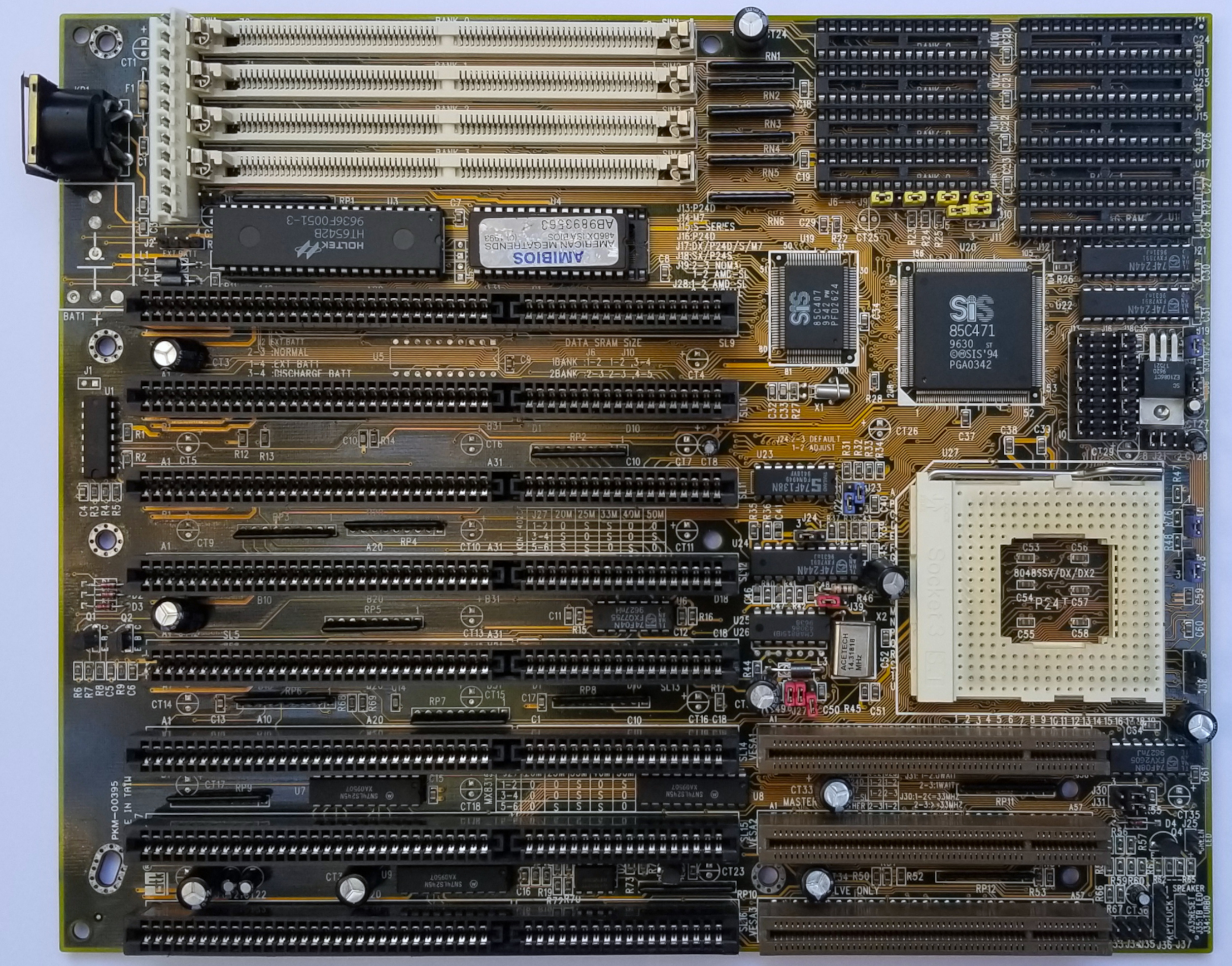
The ALD PCI 5433 is a based on the single chip ALD 93C488 chipset, and boasts numerous features that sound to be little more than marketing fluff. One such feature is the "latest Pentium class technology...Pipeline Burst Synchonous SRAM Cache...," which happens to distinguish this fellow as the only known 486 board with pipeline burst L2 cache. This made such an assembly quite interesting, as it raised numerous other questions, such as: How flexible is it? How true is the claimed PCI 2.1 compliance, and how is its PCI implementation in general? Is the ALD 93C488 something that happens to be re-labelled, or is it truly an in-house single-chip 486 solution with all the bells and whistles, from WB L1 support to pipeline burst cache support to even EDO support?
Well, it's probably best to sum these answers in a few words: yes and no. Yes, it's an interesting board and, comparatively, it is decently fast. To say that it is speedy is a stretch; it's probably in the lower tier of SiS496/UM8881 boards, and that might be the whole story for you right there. However, as they say, there's always more to the story-and with this ALD fellow, there certainly is. I suspect that more can come of this assembly in the future.
As to the other questions, let us examine them one-by-one:
- It's not that flexible. It is certainly fast as far as PCI throughput, but that's about where the fun ends. Pipeline burst L2 should in theory support higher FSB speeds, but the silicon driving the assembly seems to be rated at a cap of 40MHz. That's not great, as pipeline burst cache loses out to asynchronous cache as far as timings go, at least at slower speeds. It is the scalability and speed at scale that makes pipeline burst L2 desirable; neither of those facets of operation is found here.
- The PCI implementation can be characterized as "okay." It is not bad, speed-wise, but the sheer bus throughput is not enough to overcome the limitations of the chipset. Yes, it appears that the PCI implementation is marginally faster with respect to bus transfers than the SiS496 and UM8881F chipsets. That's not precisely saying much as, again, the story with those boards, as shown by pshipkov and Feipoa, amongst the others here, is speed at scale. The UM8881F chipset really comes into its own at 60/66MHz, as does the SiS496. It's a shame to say that the ALD 93C488 probably would be on par with those fellows at said speeds, but its design is inherently limited by the market segment it was meant to target.
- Yep, the ALD 93C488 appears to be its own thing. That's neat.
This board has driven me positively mad; the otherwise standard AMI WinBIOS is obscenely complicated, with numerous features not exposed on most other "normal" boards facing the end user. There's listings for numerous configurable options, some of which prove interesting, and others of which prove absolutely confusion-inducing. I have provided a few pictures below to elucidate the point at which I am trying to reach; that this board, at its very core, is absurdist. The manual explicitly notes, "For optimization purpose[sic], most of the BIOS parameters have been pre-determined[sic] by the manufacturer." They are not even close to joking. Changing even more than a few of the BIOS settings from the "Optimal" configuration setting can hang the board in BIOS. I found the most stable changes that improved performance to be as follows:
STAGGERED REFRESH MODE = ENABLED
REFRESH MODE TIMING = 1 CLK
RAS PRE-CHARGE TIME = 3 CLKs
RAS ACTIVE TIME = 3 CLKs
FAST MODE READ CAS ACTIVE TIME = 1 CLK
PCI/ISA MASTER EXTRA WAIT-STATE = 0WS
PCI WRITE BUFFER = ENABLED
HOST ADDRESS/DATA XFER SPEED = FASTEST
ISA FAST DMA CYCLE = ENABLED
PCI/ISA MASTER READ WS = 0ws
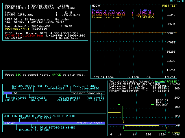
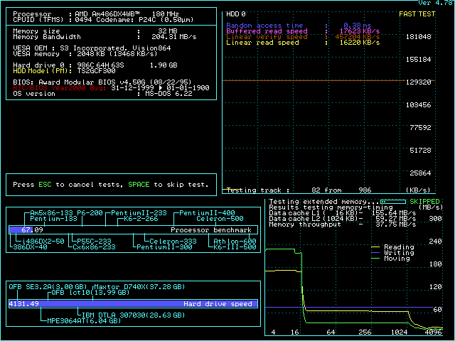
There are two cache arrangements: Flow Through and Pipeline. I have results with both attached below. Flow Through seems slightly faster, and that's the story with that. Further, it's worth noting that EDO support works, which is nice. It is pretty flawless, unlike with some other 486 boards. The onboard IDE is very decent; it is an LGS Prime 3Bit is seemingly integrated into the chipset, like with the Intel Aries. The LGS Prime 3B is an ISA-based Super I/O controller. My bad! With a CF card, it seems to offer very fast speeds in DOS, and no driver is required. Undoubtedly, that is a large plus, for when conventional memory needs to be prioritized.
Does anyone know what the difference is here, as far as Flow Through and Pipeline are concerned? The manual and chipset databook are silent as to this.
This board notably supports 25MHz FSB, 33MHz FSB, and 40MHz FSB. I am not certain if this ALD single-chip chipset can support 50MHz FSB, and would be rather inclined to believe that it probably cannot. The integration of this hardware is notably tight, so much so that it suffers greatly at the expense of its design. It is not per se a bad design, but ALD certainly marketed this board as a cheap non-Pentium alternative. The date code of 1996 probably support this fact, and I would not mind staking a claim that this board served as ALD's low-end offering. They did have some Pentium boards, and even those are comparatively cheap when placed against other manufacturer's assemblies; that being said, there's no doubt in my mind that this board was not made by a premium manufacturer. The PCB is somewhat cheap, and I am positive that the keen-eyed amongst you has noticed the superficial damage to the lower-right corner. This guy had a hard life, and the truth could not be any simpler than that. Sometimes, I find this board a bit cranky and unwilling to POST; that is usually after hard-locking it from what it probably cosniders to be gratuitous attempts at changing the BIOS settings.
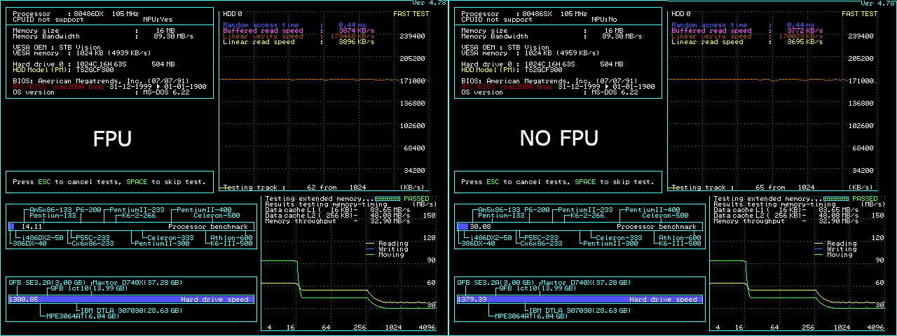
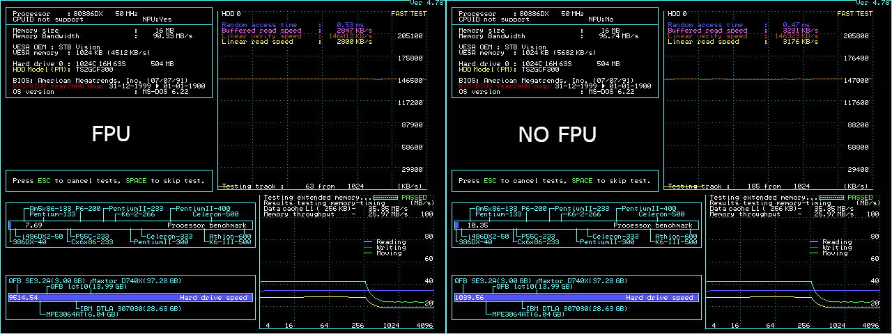
For the tests, I utilized the following configuration:
- Am5x86 at 160MHz
- WB L1 cache
- Flow Through and Pipeline L2 cache
- Matrox Mystique (which should be about the same as pshipkov's Millenium, as far as DOS is concerned)
- 1 x 32MB 60ns EDO SIMM
- 512MB BR&TD CF Card
Results follow below. DOS performance was enough for me to call an audible on this one as far as further testing goes. I can provide performance numbers for Windows if so desired, and I can try 3D rendering, but it seems to me that this assembly is just too far out there to be worth examining further. It is undeniably very cool and fast enough that it makes some sense to use, but it is not nearly as exciting as the LSD or UUD boards.
I can test other cards/settings as desired. The slough of aforementioned crazy BIOS settings is attached here; if someone has any suggestions about where I can start tightening things up further without losing stability, I am all ears.